Topic: 8085 SBC rev 3 VCF East XIII Special Edition
Date: 2018 JUN 30
Quick Links
Introduction
It’s been around eight years since my first 8085 SBC writeup, and just under seven years since the second revision 8085 SBC. I’d been planning a third revision for some time. The rework and layout even got started once before, but derailed and never came to completion. Several of us had discussed doing a new SBC for VCF East XII in 2017, but there wasn’t enough time to get a new revision designed, prototyped, and kitted up before VCF East, so we did an XT-IDE workshop instead. This year, we set the design goals and got started early:
- True single-board computer: no extra add-on cards necessary for basic operation
- Monitor in ROM
- 8085 based, an extension of the existing 8085 SBC designs
- Serial console
- Expandable
- Potentially able to run CP/M
- BASIC in ROM would be nice
- No hard-to-get parts
- Single 5V supply
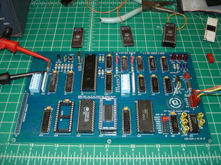
The 8085 SBC rev 3 meets all of these goals. Additionally, it allowed me to introduce Glitchbus, a generic 8-bit bus I’d been planning since at least November 2010. Here’s a picture of the first prototype board, which worked first-try:
Basic SBC Design
The 8085 SBC rev 3 is implemented in a single 5x8 inch double-sided PC board. It incorporates the following:
- 8085 CPU clocked at 2 MHz (overclocking possible)
- 64KB static RAM
- 32K ROM
- 8251A USART for console serial port
This is a direct extension of the 8085 SBC rev 2. Rather than expecting 32K RAM and 32K ROM, with ROM starting at 0x0000, this revision uses a ROM banking scheme and a ROM boot circuit. ROM appears as a 4K page at a switch-selectable base address (default of 0xF000). The 4K page mapped in is selected using four bits of an I/O register. One element of a 74LS74 flip-flop allows ROM to be enabled or disabled under software control, so that the full 64K of RAM can be used after bootstrapping. Additionally, the second element of the 74LS74 controls “ROM boot.” When enabled, ROM appears at all memory addresses, repeating every 4K. This allows the 8085 to execute code from ROM when it resets to 0x0000. The boot code can then jump into the ROM’s actual address and switch off boot mode.
The 8251A UART was chosen for a console since it is a relatively simple, cheap, and easy to get device. While the Multi-IO board used a Zilog SCC, some builders found the SCC too complicated and voiced a preference for a simpler UART that required less initialization. Being part of the MCS-85 family, the 8251A is a solid choice for an 8085 SBC, anyway!
All glue logic is implemented using standard TTL logic, there are no programmable logic devices (GALs, PALs, CPLDs) involved.
ROM Considerations and ROM-FS
With the goal of having both a ROM monitor and BASIC in ROM in mind, I started considering how ROM would be laid out. Since the board was to potentially use EEPROM, I’d wanted to provide a mechanism for in-board programming: this would allow easy updates to operating software without access to an EPROM programmer. There were extra DIP switches available in the design, so it’d be nice to be able to select the monitor or BASIC from switches, rather than always going to one or the other.
After experimenting with a number of solutions, I decided to implement a ROM filesystem. While ROM-FS will be fully documented later, it basically allows records of up to 256 blocks of 128 bytes to be stored in ROM. There’s a directory at the beginning of ROM-FS, which allows for numbered and named records. Having the records numbered meant that one of eight possible records could be selected via the three spare DIP switches for booting. I ended up including the load address and entry point in the directory, so that code from ROM-FS could be loaded anywhere in memory and jumped to.
This also has another huge benefit: there can be multiple copies of the same or similar records in ROM-FS. For instance, one can upload a newer version of the ROM monitor to a new ROM-FS record, keeping the old one, but selecting the new one as the default boot record via DIP switch. Updates to the board’s firmware are thus far less risky!
Console Serial Port
While the choice of the 8251A USART for the console device was easy, there was some question as to how it should interface to the outside world. Should it be USB, providing both a USB serial port and power over one cable? Should there be provisions for pluggable transceiver modules to allow things like 20 mA current loop? If we go with RS-232, which type of connector should be on the board? How should be bitrate be selected?
To allow maximum flexibility, we decided on RS-232 signalling via MAX232 level shifter (keeping the single 5V supply), and stuck a 5-pin Molex KK-100 connector on the board. Kits are provided with a pre-crimped pigtail that mates with the Molex connector but has no connector soldered to the other end. This allows the assembler to choose the termination. This seems to have worked well, and the use of a KK-100 connector means that we can design a USB interface board that plugs on, but doesn’t restrict the board from use with classic RS-232 serial terminals.
Bitrate selection ended up being via jumper header. A local bitrate oscillator was provided, using a 2.4576 MHz crystal and binary counter IC. This also keeps the serial bitrate separate from the main system clock, meaning that the CPU can be overclocked without disturbing serial timing. Indeed, at least one user has taken their 8085 SBC up to 6 MHz at the time of writing!
Expansion
Many people seemed to like the PC/104 style stacking expansion of previous 8085 SBCs, so it was decided that this interconnect method would stay. Rather than stick with a multiplexed expansion bus that was essentially the 8085 pins brought to a connector, I took the opportunity to implement an idea for a processor-agnostic expansion bus I’d been thinking about since at least November 2010. This bus, which folks on IRC started referring to as “Glitchbus,” takes its inspiration from having worked with many different vintage 8-bit busses and comparing their strong points and shortcomings. The signal lines aren’t tied to the timing of any specific processor, instead being based off of a *BSTART signal. The feature set included is complete enough to be useful (really only lacking DMA), but minimal enough to be easily implemented with almost every 8-bit processor available.
A future writeup and interfacing guide for the Glitchbus will be available, a link will be added here when it’s finished!
VCF East XIII Special Edition
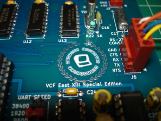
This board was really designed for, and initially released at, VCF East XIII, May 2018, at the InfoAge Science Center in Wall, NJ. I was provided with a high-resolution image of the official VCF logo, which I was able to work into a format suitable for PC board production. I think it turned out great:
All in all, 36 8085 SBC rev 3 kits were sold at VCF East XIII. Most of those were assembled during the event. Everyone who assembled one went home with a fully functional single-board computer, most of them worked on first power-up! By far, the biggest issues encountered were, in order of frequency: missed solder points, solder bridges, and cold solder joints.
If you’d like to build your own 8085 SBC rev 3 board, please contact us – kits will eventually be up in our Tindie store, but are not currently up. Board files for the generic, non-special-edition version will be published on GitHub.
SBCs built

