Topic: Designing and testing an 8085 SBC
Date: 2010 SEP 02
Update 2018 JUN 30
You probably want to head over to the 8085 SBC rev 3 writeup if you’re looking for a board to build. It’s a better SBC and comes with a manual! We’re offering bare boards, parts kits, and assembled/tested SBCs for the third revision.
Update 2016 MAY 18
I thought the EAGLE files for this project had been lost, but recently recovered them from backup disks. They have been uploaded to GitHub and released under the GNU GPL v3 license for free use.
I’ve wanted to build an 8085-based computer for quite a while – ever since I found an 8085 processor in an old piece of AT&T PBX equipment and read about what it could do. It’s binary compatible with the 8080, only requires a single +5V supply, and the only required support chip is an 8-bit latch. The idea of the project came and went, and was largely superceded by the use of Microchip PIC microcontrollers. In December 2009, I finally decided to build a prototype 8085 single-board computer, as my I/O needs were outgrowing the midrange PICs.
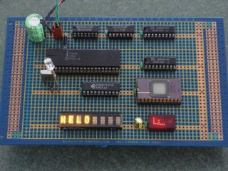
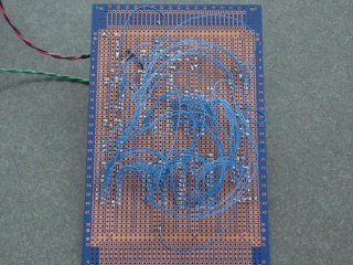
The prototype consisted of a Vector protoboard with all of the ICs mounted in sockets and soldered down to the traces. Connections were made largely with #30 Kynar wrapping wire, soldered point-to-point rather than wrapped. The prototype utilized a 2716 2K x 8 EPROM for program storage, and two 2114 1K x 4 static RAMs for stack and variable space. Address segment decode was done with NOT and NOR gates as combinational logic. The low address byte was demultiplexed using a 74LS373 8-bit latch.
In addition to the memory devices and glue logic, there’s also a PDSP-1881 character display attached to ports 0-7. It shares port 0 with the TIL311 hex display, which was initially added for testing, but left since it was already wired in. Writing ASCII characters to ports 0-7 causes them to be latched and displayed on the PDSP-1881. If you’re going to use one of these character displays, I found it useful to tie its clock input line to the clock output of the 8085.
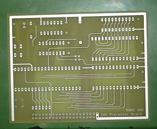
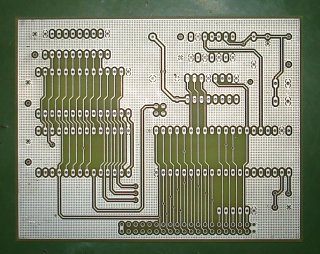
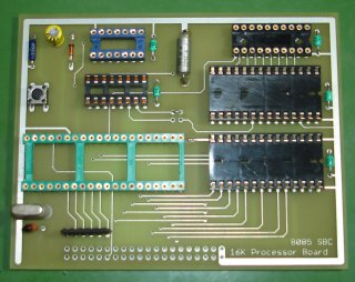
While this design proved useful for playing with devices requiring true address and data buses, such as character displays, the prototype was cumbersome to expand. The point-to-point soldered connections tried to unsolder themselves whenever you heated a joint to add another wire. My initial decoding scheme for memory devices didn’t leave room for easy expansion. Since I was also beginning to restore a Cromemco Z-2D at the time, I decided to eventually lay the prototype out as a real PCB and have one etched at a fab house. I kept my design within the 4x3” size restriction in the Lite version of CadSoft’s EAGLE – not only because I didn’t have anything else, but so that anyone wishing to build the project could edit my files and design stacking expansion boards without having to purchase a CAD package! Eventually, the board got produced by PCB-Pool, and arrived at my door from Ireland:
PCB-Pool did a fine job, and they will accept EAGLE files directly, so no worries about conversion to Gerber files. They also provide you with images of your PCB at each stage of its production, free-of-cost. If you include any SMD components, they will also give you a stainless steel laser-cut paste stencil, for free. They do offer solder mask and silkscreening for an increased price, but I prefer unfinished boards for prototypes, since it’s easier to modify tracks.
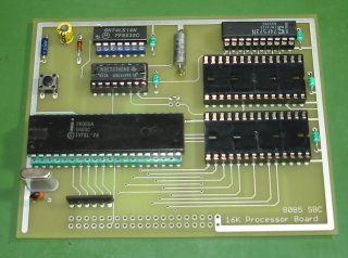
I installed the IC sockets and various discrete components first. These include the oscillator crystal and its capacitor (lower left), the reset circuit (capacitor, resistor, diode and tact switch in the upper left), the tantalum capacitor serving as main power supply bypass (silver tube top center), and the smaller 0.1 uF bypasses scattered around the board (blue-green beads). There’s also a 1Kohm x 5 resistor pack near the bottom of the board, and this holds various interrupt/hold lines down.
Then the sockets get stuffed with various ICs. The big one is, of course, the Intel 8085. This particular 8085 is the “A” revision, but an actual Intel part. The first IC above the 8085 is a 74LS138, which decodes the top three address bits into 8 select lines for memory devices – the first two outputs are mapped to the ROM and RAM. The 74LS138 also depends on the 8085’s Memory-I/O status line, which keeps the memory devices from responding during an I/O read/write. The IC above that is a 74LS14 Schmitt hex inverter, which forms part of the reset circuit. The final small IC is the 74LS573, which is an 8-bit-wide latch. This is needed to latch the multiplexed low address bits off of the address/data bus.
The reset circuit itself bears mentioning, as it is simple but effective. It consists of a capacitor, charge resistor, shunt diode and the tact pushbutton. On power-up, the capacitor is discharged due to the diode, so the system is put in reset. It charges through a 10K resistor, allowing for a nice, wide reset pulse. It serves double-duty though, because the tact switch in the circuit will also shunt the capacitor’s charge to ground when it closes, so it provides both power-up reset and debouncing/proper pulse width for the reset pushbutton.
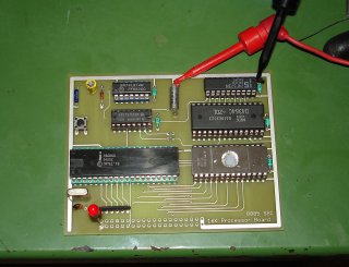
Time to test the board! One nice thing about the 8085 is the inclusion of the SIO pins SOD and SID. These are single-bit input and output pins, often used for on-chip serial communications when the 8085 is used in an embedded application. You can attach an LED with a dropping resistor to the SOD pin (pin 4 of the 8085) and turn it on and off through software – a quick and easy test to see if your ROM is being read. I expanded this with a short 8080 Assembly program that toggles the SOD pin on and off. It does so slow enough that an attached LED will flash slowly. I wrote the code using a function call to the delay loop so that I might exercise the RAM through the processor’s stack:
;Flash a LED on SOD
;Top of RAM @ 0x4000

START:  LXI H, 4000h
        SPHL

FLASH:  MVI A, 0C0h
        SIM
        CALL DELAY
        MVI A, 40h
        SIM
        CALL DELAY
        JMP FLASH

;Delay, return to HL when done.
DELAY:  MVI A, 0FFh
        MOV B, A
PT1:    DCR A
PT2:    DCR B
        JNZ PT2
        CPI 00h
        JNZ PT1
        RET
It was assembled with GNUSim8085 and manually programmed into my Intel iUP-201 PROM Programmer. The test code was first run in the original point-to-point prototype, to ensure my code was correct! After re-burning it to a 2764 EPROM, it worked fine in the new PCB:
If you’re interested in producing one of these PCBs yourself, check out the project files directory for layout files, schematics, notes and software. If there’s enough interest, I would consider doing a larger run of boards and providing bare boards and/or kits for individuals. Contact me using the contact link in the page header.
