Topic: Intel 8085-based SBC, Revision 2
Date: 2011 OCT 29
Update 2018 JUN 30
You probably want to head over to the 8085 SBC rev 3 writeup if you’re looking for a board to build. It’s a better SBC and comes with a manual! We’re offering bare boards, parts kits, and assembled/tested SBCs for the third revision.
Update 2016 MAY 18
I thought the EAGLE files for this project had been lost, but recently recovered them from backup disks. They have been uploaded to GitHub and released under the GNU GPL v3 license for free use.
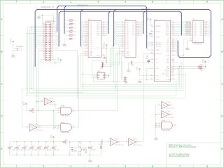
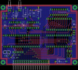
After discussing the 8085 SBC with John Wilson of D-Bit, I decided to revise my SBC board layout. The changes are significant, but do not break compatibility with the original SBC design, though the original design does require a few modifications to make it more or less software and hardware compatible with the second revision. Here’s the full schematic for the Rev. 2 board, along with an image of the board layout:
The biggest change in the second revision is in the onboard memory devices: the second revision board now supports a full 64K of memory on-board! The board is arranged in a similar way to the first revision, with a static RAM in the top 28-pin socket and a ROM in the bottom socket. This revision uses a 62256 32K x 8 SRAM for system RAM. The lower “ROM” socket is jumper selectable for 8/16/32K EPROM or EEPROM or a second 62256 SRAM. Since the /WR line is provided at the socket, it should be possible to use SRAM, EEPROM or FeRAM at this location, making it possible to write a ROM monitor that can update itself in-board.
With the possibility of the entire memory address space being filled by on-board devices, I decided to include a bus signal to disable the onboard memory devices. This is present as /MASK on pin 12 of the expansion connector. It’s pulled up on the SBC since it is active low. When pulled low, it disables both of the NAND gates that make up the memory address decode circuit, allowing external memory devices to map part (or all, if one so desired) of memory space. While this isn’t as useful in the context of an embedded SBC, it does allow for the possibility of the use of the 8085 SBC as the base building block for a full system; for example, a small CP/M box.
Aside from the changes to the SBC’s memory structure and decode circuitry, I brought the RES_OUT signal from the 8085 to the bus, on pin 11 (rather than pin 4 as seen in the Scrolling LED Display Writeup), thickened the traces to 0.16”, and added two Molex KK-100 headers at the top edge for power and external reset. These connectors should make it easier to use the 8085 SBC as the base board in a stack. I also pulled up /RD and /WR for use with non-volatile writable memory devices (battery-backed SRAM, EEPROM, FeRAM, et c.). Another power supply bypass tantalum was added at the bottom of the board, next to the expansion connectors. Possibly the most important mechanical change is the addition of 1/4” corner mounting holes to permit PC/104 style board stacking!
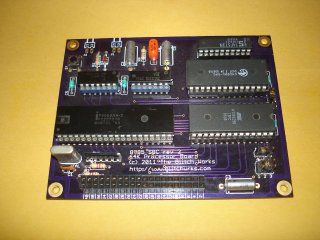
I broke with tradition on ordering the prototype board for this run, and switched from PCB-Pool to DorkbotPDX’s PCB Order Service. They offer short-turnaround pooled PC board prototype runs at a low cost…a very low cost. Double sided boards are $5.00 per square inch, lead free, with solder mask and silkscreen on both sides. The $5.00 includes all setup and shipping and gets you three copies of your design. They can accept several filetypes, including EAGLE CAD PCB files. I’ve been very impressed with their service, and also appreciate that the boards are made in the USA. Here’s a look at the assembled Revision 2 prototype PCB from DorkbotPDX:
Excellent work! Although it’s not specced for their PC board orders, all of my prototype runs through DorkbotPDX have come with gold-plated pads. The purple solder mask is a bit of a change from the typical green, but looks good with gold pads and white silkscreen. These boards originally came with tabs along the edges where they’d been connected to other boards. They were easily removed with cutters and smoothed over with a small, flat hobby file. I’d definitely recommend DorkbotPDX for any small prototype boards you need!
The board is shown with a Cypress 70 nS CY62256 SRAM installed, along with an Atmel AT29C256 EEPROM. The various jumpers near the EEPROM determine a few signals that the 28-pin “ROM” socket receives, and are currently jumpered for a 32K EPROM/EEPROM. As you can see, this board was stuffed with a full-size quartz oscillator crystal…I plan on swapping it out for a short-can crystal so that it doesn’t interfere with the board above it when stacked. Speaking of stacking boards, the Serial/Parallel IO board is in the works, with a prototype already having been wire-wrapped – keep an eye out for updates on progress!
The Revision 2 prototype boards worked perfectly! After modifying the top-of-stack address for my SOD LED Flash Test and burning it to ROM, the SOD pin was observed to change state regularly with a logic probe. Success! Now to get on writing that ROM monitor…


