Topic: Serial and Parallel Multi I/O for the 8085 SBC
Date: 2017 APR 24
Wow, time flies! I started on this project in September 2011, according to this VCForums post. The production board made it to HOPE Number 9 in NYC in the summer of 2012. Finally, here’s the writeup!
Quick Links
- VC Forums Prototype Thread
- GitHub Repository for all 8085 SBC Related Boards
- GitHub Repository for the Glitch Works ROM Monitor
Prototyping an I/O Board
With the design of the 8085 SBC rev 2, I knew I eventually wanted to add an I/O board with at least a serial port for use with a ROM monitor. I had recently built a s100computers.com Serial IO S-100 Board and settled on the Zilog 8530 SCC as the choice for a serial controller: you get two serial channels in a 40 pin package, onboard baudrate selection, and each channel only requires two I/O registers. The SCC is more complex to program, but it’s well documented, and I had a working system on which to develop my ROM monitor since I already had the s100computers.com board up and going.
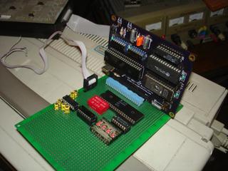
The first steps in developing an I/O board were of course to prototype it. To keep all of the prototype and SBC circuitry available for probing, I used a right angle 40 pin header on a chunk of protoboard. The final version would stack, PC/104 style, over the SBC, but having the two boards at a right angle to one another was more convenient for prototying:
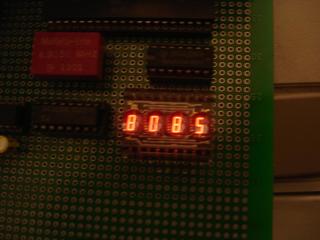
In addition to the Zilog SCC and clock generator, I also added a DL-2416 ASCII character display. These provide a convenient output for debugging. I’ve used them in many previous projects, including my S-100 Debug Board. One of the first tests of the I/O board was to copy characters from the SCC’s first serial channel to the DL-2416 display:
Developing a Simple ROM Monitor
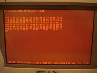
The I/O board and Glitch Works Monitor were developed in tandem, debugging with the s100computers.com board in a S-100 system until enough of the monitor was functional to self-debug. This mostly consisted of dumping new monitor binaries into the 8085 SBC’s RAM through the serial port and jumping to it, so that new EPROMs didn’t have to be burned for every change. The initial version of the ROM monitor supported the Dump command only, and auto-incremented its dump address, starting at 0x0000. Here you can see it being displayed through Procomm Plus on my Compaq Portable/386:
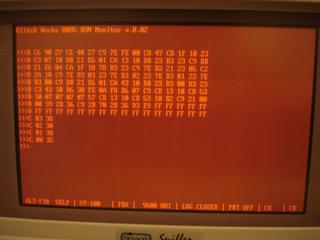
The command processor was expanded with routines to decode hex input. I followed what seemed like the simplest path for taking user input commands: read a character from the console port, see if it matches a single-letter command, and either move to handle the command or display an error message. Early microcomputer monitors like the North Star Monitor also follow this pattern, automatically inserting spaces after accepted commands. The following is a mid-development screenshot, with the Dump command still auto-incrementing a base address, but with an output command mapped as C. At this point, C XX YY would output byte YY to I/O address XX. With the 8085, this of course required self-modifying code!
The minimally workable version got labeled v0.1 and, at the time of writing, is current on GitHub. I split out the I/O modules to make it easier to customize for multiple systems. Here’s a text capture of a session with the monitor running on the 8085 SBC rev 2 with the Multi-IO board:
>Glitch Works Monitor for 8080/8085/Z80 and Compatible
Version 0.1 Copyright (c) 2012 Jonathan Chapman
Built with 8085 SBC Multi I/O module

>d 0000 0100
0000 : C3 EB 01 21 77 01 CD 6C 01 21 28 02 CD 6C 01 21
0010 : DE 01 CD 6C 01 CD FE 01 E6 5F FE 44 CA A3 00 FE
0020 : 45 CA 63 00 FE 47 CA 9A 00 FE 4F CA 3C 00 FE 49
0030 : CA 4F 00 21 E3 01 CD 6C 01 C3 0F 00 CD 66 01 CD
0040 : 25 01 47 CD 66 01 CD 25 01 CD 4D 01 C3 0F 00 CD
0050 : 66 01 CD 25 01 47 CD 66 01 78 CD 53 01 CD F3 00
0060 : C3 0F 00 CD 66 01 CD 1C 01 62 6B 3E 0D CD 0A 02
0070 : 3E 0A CD 0A 02 CD 13 01 CD 66 01 3E 3A CD 0A 02
0080 : CD 66 01 CD EE 00 CD 66 01 CD 25 01 DA 0F 00 77
0090 : CD 66 01 CD EE 00 23 C3 6B 00 CD 66 01 CD 1C 01
00A0 : 62 6B E9 CD 66 01 CD 1C 01 62 6B 0E 10 CD 66 01
00B0 : CD 1C 01 3E 0D CD 0A 02 3E 0A CD 0A 02 CD D5 00
00C0 : 7A BC FA 0F 00 7B BD FA CD 00 C3 B3 00 7A BC C2
00D0 : B3 00 C3 0F 00 CD 13 01 CD 66 01 3E 3A CD 0A 02
00E0 : 0E 10 CD 66 01 CD EE 00 23 0D C8 C3 E2 00 7E CD
00F0 : F3 00 C9 C5 47 0F 0F 0F 0F E6 0F CD 0C 01 CD 0A
0100 : 02 78 E6 0F CD 0C 01 CD 0A 02 C1 C9 C6 90 27 CE

>
Laying Out a Multi-IO PC Board
With a workable monitor and a serial console prototyped, it was time to lay out a proper stacking module for the 8085 SBC. I had originally intended to include the Zilog SCC and a Zilog CIO. The CIO included a timer/counter module in addition to parallel I/O and supported complex options like interrupt on bit pattern matching. Unfortunately, I’d decided to use PLCC ICs in through-hole sockets, and couldn’t find a pinout for the Zilog CIO in PLCC at the time. For that reason, the Multi-IO rev 0 board contains an Intel 8255 PIA. While it lacks some of the advanced features of the Zilog CIO, it is very easy to interface with, and many interfacing examples exist.
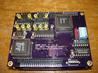
The board was laid out in EAGLE CAD as a two-layer board, again fitting within the size restrictions for the Lite version of EAGLE. It stacks above or below the 8085 SBC using the 40-pin section of a PC-104 stacking header. Here’s a veiw of the top of the board, with a Zilog SCC and Intersil-made 8255 PIA:
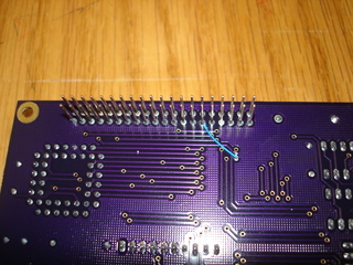
The prototype board almost worked on the first try – a single cut-and-jump patch was required. Fortunately the cut was between two vias on the bottom side of the board. This has been fixed in the layout files on GitHub:
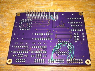
Here’s a shot of the bottom of the board. The extra green jumper wires from the 8255 PIA to one of the port headers allowed the addition of a DL-2416 display on an external bit of protoboard. This was set up at HOPE Number 9 and allowed users to have something to poke bytes into:
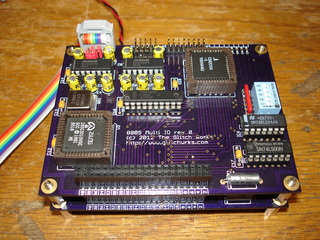
At least two other people have built Multi-IO boards and used them with their 8085 SBCs. Since the Multi-IO mirrors the functionality of the s100computers.com Serial IO board, it’s possible to use the same software with either setup with very little modification, providing your programs will run on the 8085 in both cases (no Z80 opcodes for S-100 systems!). Here’s an angled shot of the Multi-IO stacked on my personal 8085 SBC, it’s currently running the monitor session that produced the above textual monitor capture:
If you’re interested in producing one of these PCBs yourself, check out the project files directory for layout files, schematics, notes and software. If there’s enough interest, I would consider doing a larger run of boards and providing bare boards and/or kits for individuals. Contact me using the contact link in the page header.
serial ports fried
