Topic: Building a debug board for troubleshooting S-100 systems
Date: 2011 SEP 01
Whether you’re trying to bring up a S-100 system for the first time or you’re working on reconfiguring a piece of hardware for your existing S-100 box, having a way to determine the status of certain lines and the contents of I/O addresses is very handy. This isn’t a problem if you own a S-100 computer with a front panel, and can often be accomplished through a ROM monitor or debugger if you don’t. There are times, such as when bringing up a CPU board in unknown operating condition, that hardware debugging resources are essential. Since none of my S-100 systems have front panels, I’ve built a board to help in debugging low-level hardware problems.
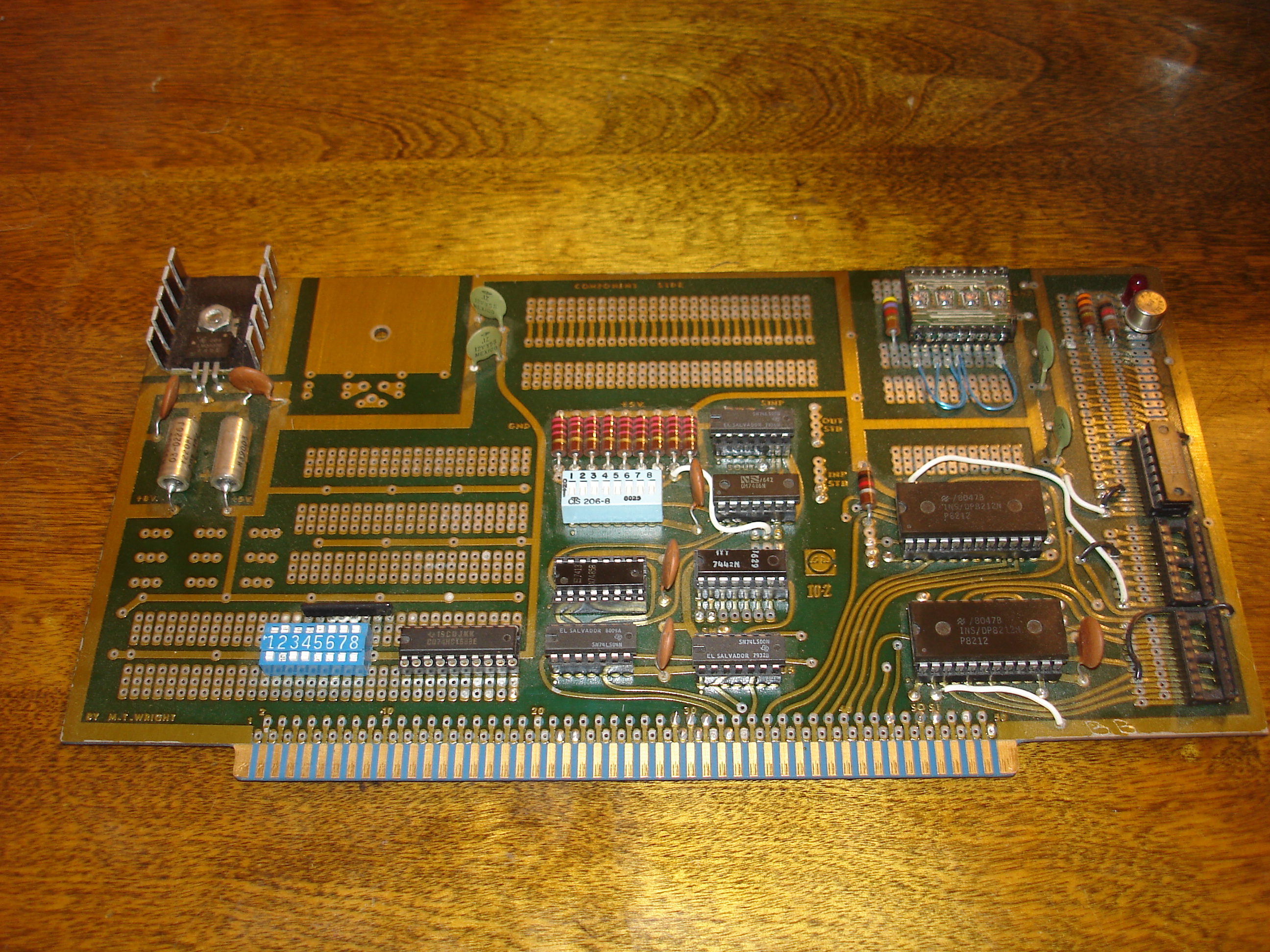
My debug board is built on a Solid State Music IO-2 board. The IO-2 is a fairly early S-100 board, and aimed to be a universal I/O and ROM solution for IMSAI and Altair computers by providing only a few fully defined functions. These are limited to address decode and a pair of Intel 8212 8-bit I/O ports. The board provides for a 5-volt regulator and decoupling capacitors, and leaves another copper pour and pads available for an additional regulator. The rest of the board is prototype area. Suggested functions with which to populate the board, as suggested by the manual, include 1702A PROM board, two additional parallel ports, or AY-5-1013 UART. The prototype areas are just that – DIP footprint pads. There is no fixed function in their layout. The manual (courtesy Dave Dunfield’s classiccmp.org page is mirrored here: Glitch Works File Dump.
The Halt Indicator
Generally, my first test with unknown hardware involves forcing a HLT instruction (0x76 for 8080-compatibles) onto the bus and observing the state of the S-100 bus HALT line (pin 48). The HALT line is pulled high when an 8080-compatible processor is in a halted state, so it’s a convenient test to see if the CPU card is generally functioning. Since none of my S-100 systems have HALT indicators, I added one to the debug board. The circuit is simple: a NPN transistor driving a LED, with the transistor’s base being driven by S-100 pin 48 through a 1K resistor. Any NPN transistor would do, but I wanted to preserve the vintage/homebrew look of the IO-2 board so I used a scavenged 2N3053 in a large metal TO-39 case. I used 1/2 Watt carbon composition resistors since they matched the other resistors on the board. The LED current limiting resistor is a 330 Ohm, but the value isn’t critical as long as it provides appropriate current limiting for your LED.

ASCII Character Display
My second addition was an ASCII character display. I chose a DL-2416, since I have quite a few on hand. These displays are especially simple to interface, being as they require only a 7-bit ASCII character on their data lines, two address lines to select the character, and a few logic lines to select the chip and pulse the write line to store a character. Having such a device attached to the S-100 bus is useful for checking higher functions of a CPU board – by writing code to an EPROM to output characters to a specific port, we can check the address and data buffers, as well as exercising the system stack if we choose to use a subroutine call. I have several EPROMs with these various functions programmed for debugging newly arrived, newly built or faulty S-100 systems.

Additionally, I designed my character display’s address decode circuitry to allow for disabling the display and disabling the decode comparator. The former just de-asserts the chip enable for the 74LS688 comparator and the DL-2416 display. The latter ties the active-low output from the 74LS688 low, thereby allowing the character display to respond to all I/O writes rather than a single 4-byte block. This function is useful when determining what a monitor ROM is trying to do, or in trying to determine where a monitor/hardware combination expects to find a UART. The previous revision of my debug board was put to such use in getting a Vector Graphic ZCB to load the NorthStar ROM monitor.
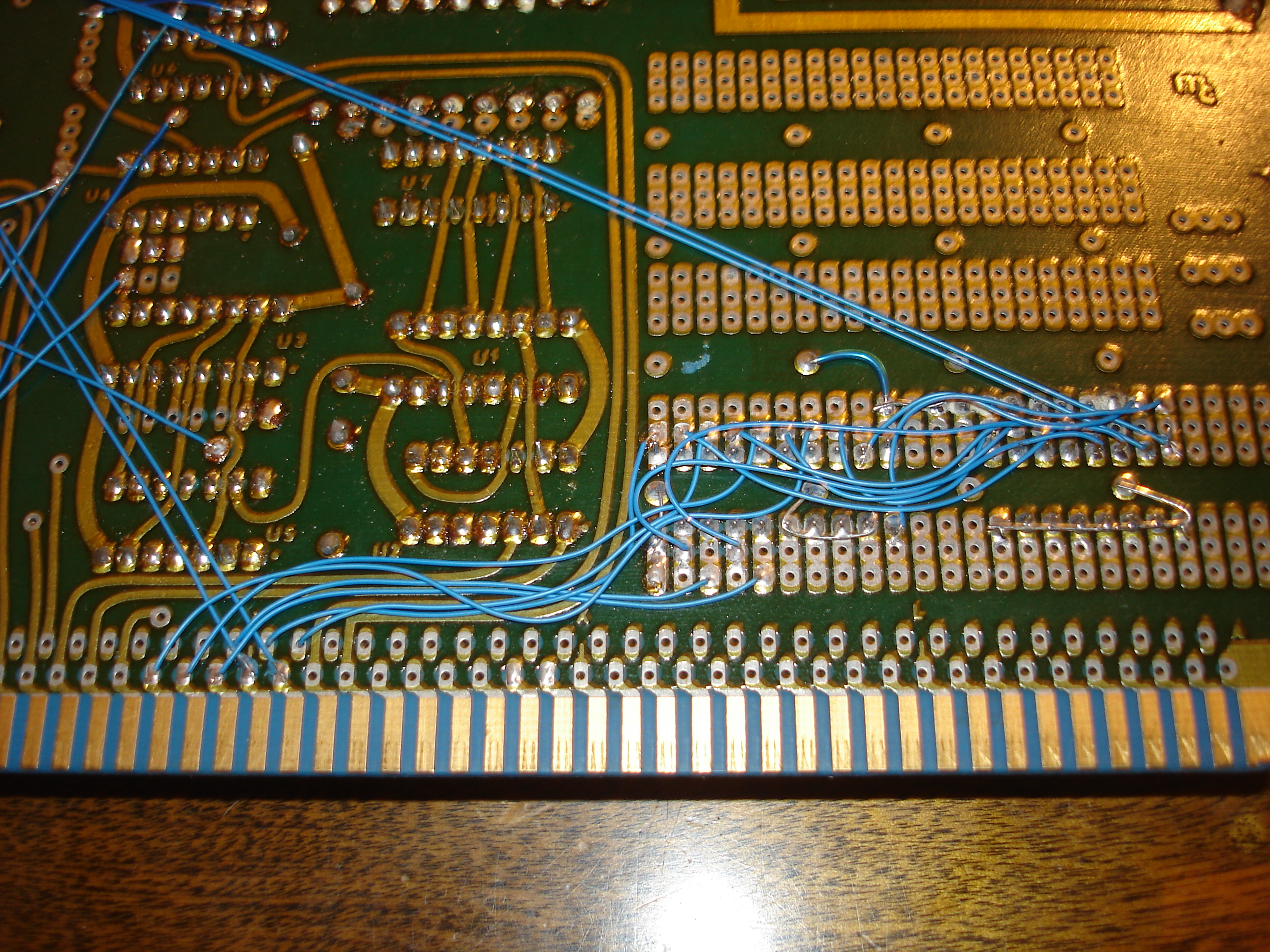
The only “modification” to the existing IO-2 circuitry required for the addition of a display was inverting the OUT STB signal from the IO-2’s built in address decoder. This was done using a spare NAND gate from the 74LS00 in the top-right corner of the address decode area. The inverted OUT STB signal was fed to the DL-2416 /WR pin. When the chip select inputs are asserted, a pulse from OUT STB will cause data on the Data Out bus to be latched in the DL-2416 display, and its ASCII representation will be displayed on the selected digit. The display’s A0 and A1 lines are tied to the S-100 bus A0 and A1 pins (79 and 80, respectively). While it is possible to use the upper address byte for I/O selection, it’s best to use the lower address byte since all S-100 boards support it, but not all boards correctly mirror the I/O address onto the upper byte.
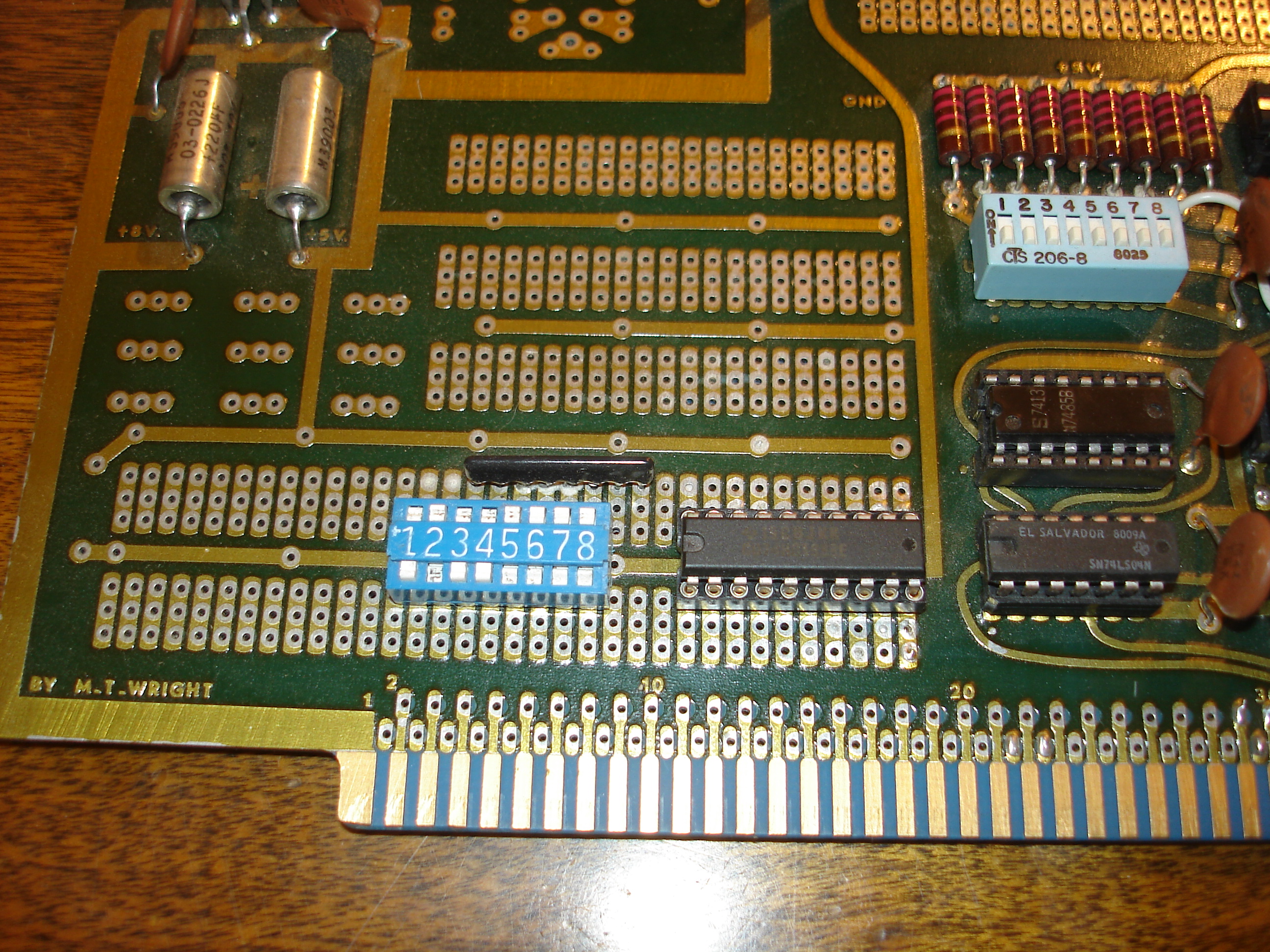
Address decode for the display is simple. A2 - A7 are fed into a 74LS688 comparator and compared against the setting on the last six positions on a DIP switch. When there is a match, the /(P=Q) line is pulled low. This line is attached to /CS1 of the DL-2416. As long as /CS2 is also pulled low (in my case, it’s wired to switch 1 of the DIP switch and pulled up with a 4K7 reisistor) and the control lines of the display are set properly (tie /CLR, CUE to ground and /CU, /BL to +5 for basic operation), data will then be written when OUT STB is asserted. In my build, the second switch in the 8-position DIP switch can ground /CS1, which causes the DL-2416 to appear at every 4-byte boundary of the I/O address space.
Native Functions: the IO-2 Byte-Wide Ports
The IO-2 provides etched traces for two Intel 8212 8-bit Input/Output ports. These ports can also be used in debugging S-100 boards, as they require no commands to start sending or receiving data. Their input and output lines are brought out to two 16-pin DIP footprints on the edge of the IO-2, which are intended to be fitted with DIP sockets for use with 16-conductor ribbon cables. A breakout box with eight toggle switches and eight LEDs would provide a simple I/O interface for the S-100 bus, and could be incorporated as function selection and output results for a diagnostic program in ROM. I plan on building such a box for my IO-2 debug card at some point in the future. Check back for updates! Future Features There are several features I’d like to add to my debug board. I’ve considered adding 256 bytes of RAM in two 2101 static RAMs, as this would also allow me to test the small quantity of 2101s I have before using them in other projects. I would also like to add a socket for a 1702A EPROM, since I don’t currently have any S-100 boards capable of reading 1702As. Both of these tasks should prove trivial, but have not been implemented as they’re not urgent.
I’m also keeping an eye out for another IO-2 board, in any condition. I’d like to build one up as a full-time 1702A PROM board. If you’ve got one you’d like to donate or sell, please contact us using the link above!