Topic: First dedicated expansion board for the 8085 SBC rev 1
Date: 2023 JUL 20
With the 8085 SBC rev 1 cleaned up and a test backplane designed, I could now lay out some boards to work with the SBC. The first board ended up being called the System Interface:
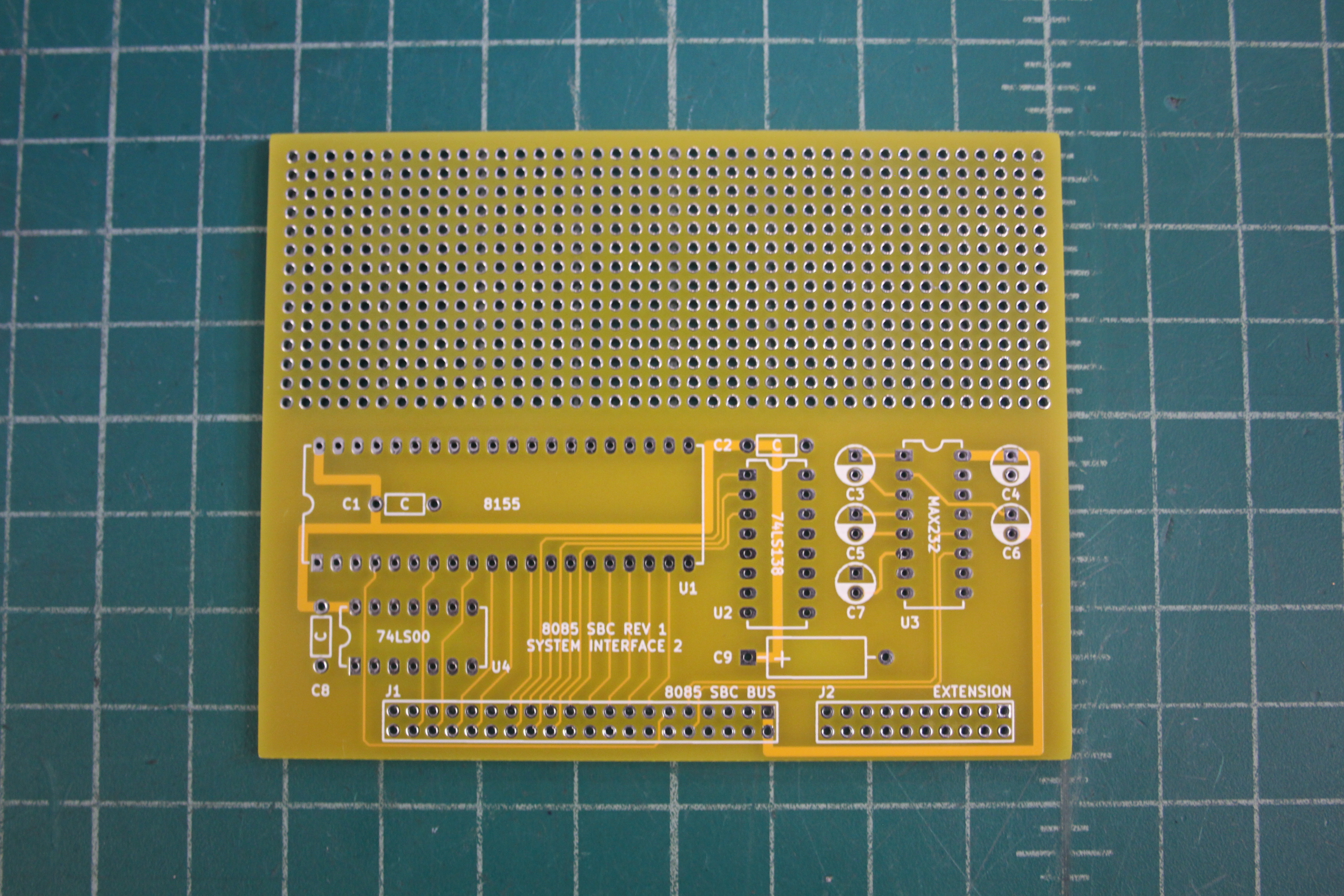
Above is the first prototype. Note that it is called SYSINT2: the first System Interface board never fully made it out of the design stage before I decided to abandon it and drastically change the board. I saved the project files in case I changed my mind, which is why this one is the “second” System Interface, despite the first one not actually existing as a board!
SYSINT2 was designed to provide the following:
- RS-232 level shifting for bit-bang serial on the 8085 SBC rev 1
- I/O address decoding for itself and other boards
- General purpose parallel I/O
- Prototyping space (approximately 50% of the board)
Originally, I’d imagined a board with a bunch of discrete read/write registers for the parallel I/O needs. Part of that was to be devoted to a hardware assist RS-232 handshake to improve the performance of the 8085’s bit-bang serial. After working on the schematic for a little while, I decided that wasn’t a very flexible way to go about it. I wanted to be able to use SYSINT2 for possibly multiple projects, not dedicate it to the intended project for the 8085 SBC rev 1.
RS-232 Level Shifter
RS-232 level shifting is provided by a MAX232 and associated capacitors. It is hardwired to pick up SID and SOD from the 40-pin expansion connector. RS-232 level signals are routed to the 20-pin expansion connector. CTS and RTS are present, as well as the TX and RX lines, so that hardware flow control can be implemented, if desired.
Conveniently, one can also steal a few milliamps of +/-10V from the MAX232, if something in the prototyping area requires it.
I/O Address Decoding
I/O address decoding is provided by a 74LS138, which generates eight active-low I/O selects, each covering 32 addresses. Fine-granularity I/O decoding is neither necessary nor desirable for the kinds of applications I was wanting to use SYSINT2 in, and would only add unnecessary parts to the BOM with no gain in utility or performance. It’s also still possible for individual boards to decode their own addresses for special cases.
One I/O decode is used on the SYSINT2 itself, for the Intel 8155, and the other seven are routed to the 20-pin extended connector. This allows jumpering I/O decode signals generated on the SYSINT2 to other boards on the backplane.
Parallel I/O
Rather than an assortment of TTL logic, latches, and buffers, I decided to use the Intel 8155 for parallel I/O. It is a MCS-85 family chip that includes RAM, three parallel I/O ports, and a timer. Since this bus is pretty much locked to the 8085, it made sense to take advantage of some of the MCS-85 family chips I’d accumulated that were intended for use with the 8085’s multiplexed bus.
The 8155 also contains RAM, and since the I/O decoder is limited to just I/O accesses, one of the six unused memory selects from the modified 8085 SBC rev 1 is used to address the 8155’s 256 bytes of RAM. The RAM is of course repeated through the 8K segment. This memory segment select is combined with the I/O select using one element of a 74LS00 quad two-input NAND.
Debugging and Using the Prototype
Prototype #1 of SYSINT2 contained a schematic error that swaps address lines A15 and A13 going to the 74LS138 1-of-8 decoder. This didn’t affect the hardwired I/O address of the Intel 8155, since it was at the top of I/O space, but caused confusion during testing. I wrote up an ECO to document the fix:
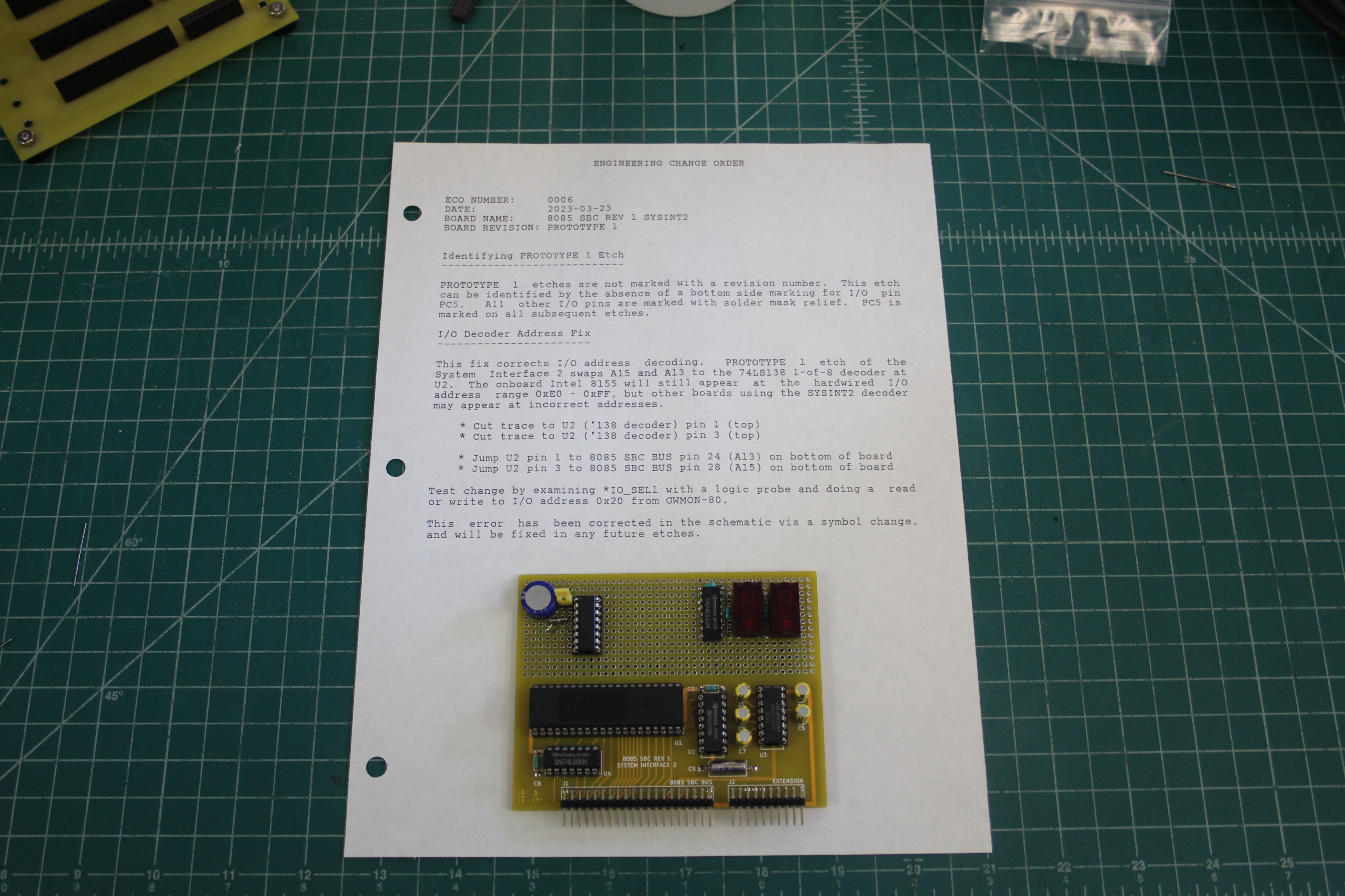
I’ve started doing this for personal projects as I always end up having to reverse engineer my own work years later. Putting a printed ECO in the binder with a copy of the schematic that accurately represents the prototype etch has proven very helpful.
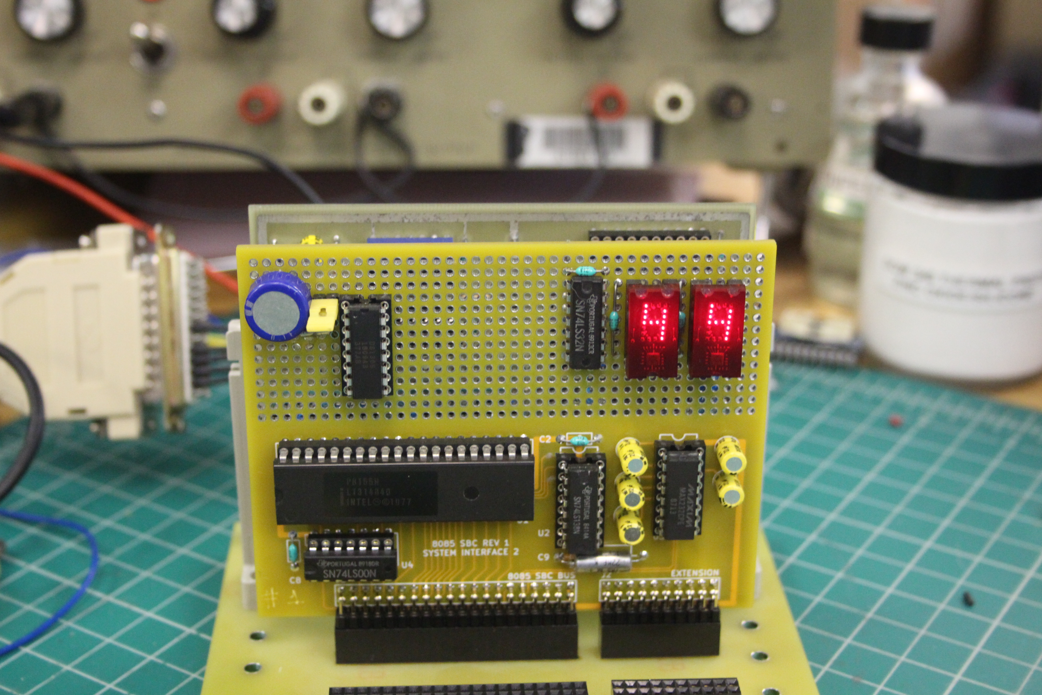
There’s a bunch of stuff on the board at this point:
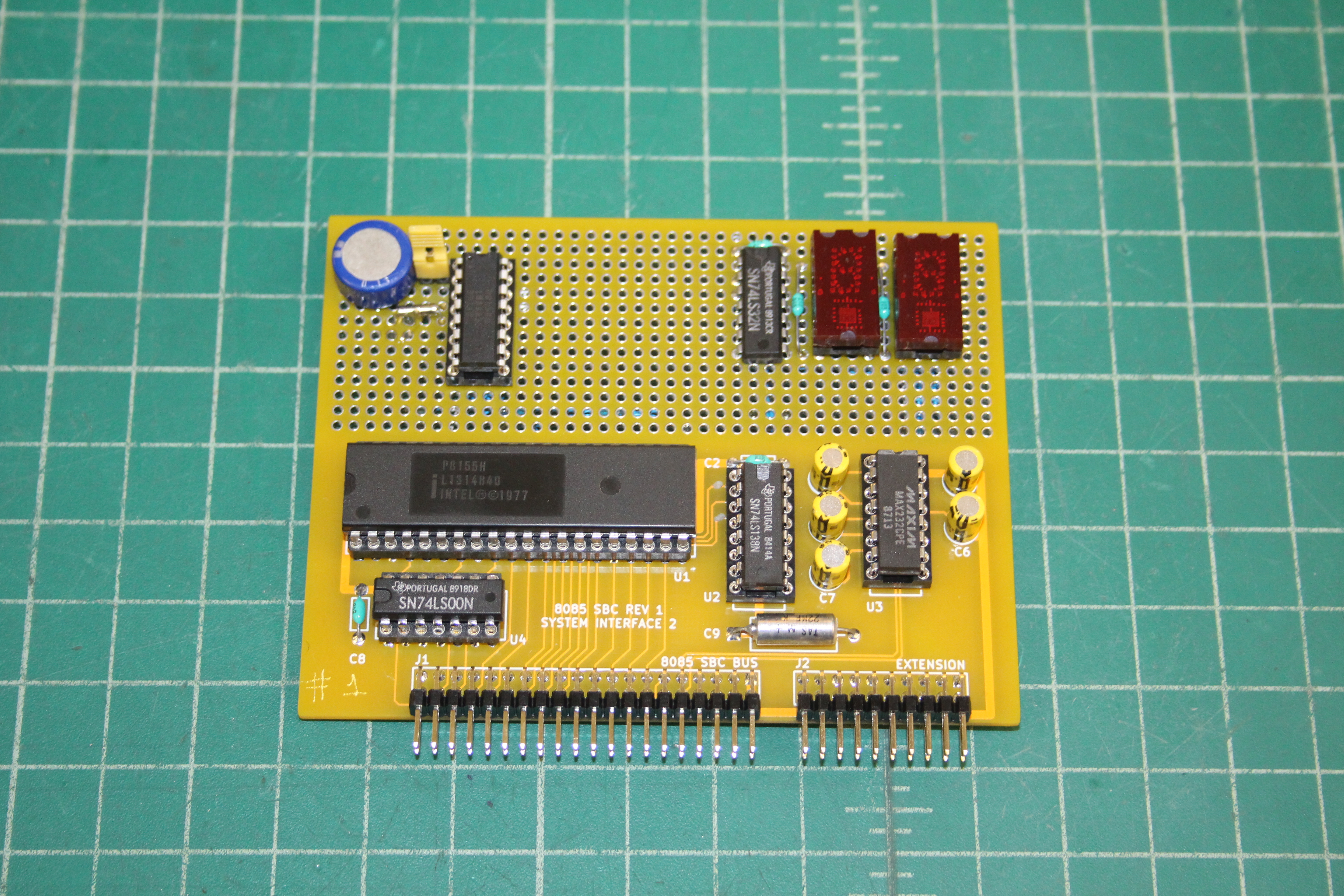
During testing, I was unable to talk to the I/O section of the Intel 8155. As part of the debug process, I added a pair of Texas Instruments TIL311 displays. These are hex decoded smart displays, which contain an onboard chip to drive the LEDs with the hexadecimal values 0 through F. They take four bits of input, and can latch the data, so they can sit right on the 8085 SBC’s expansion bus. They use one of the I/O decoder segments and an OR gate to generate their latch signal.
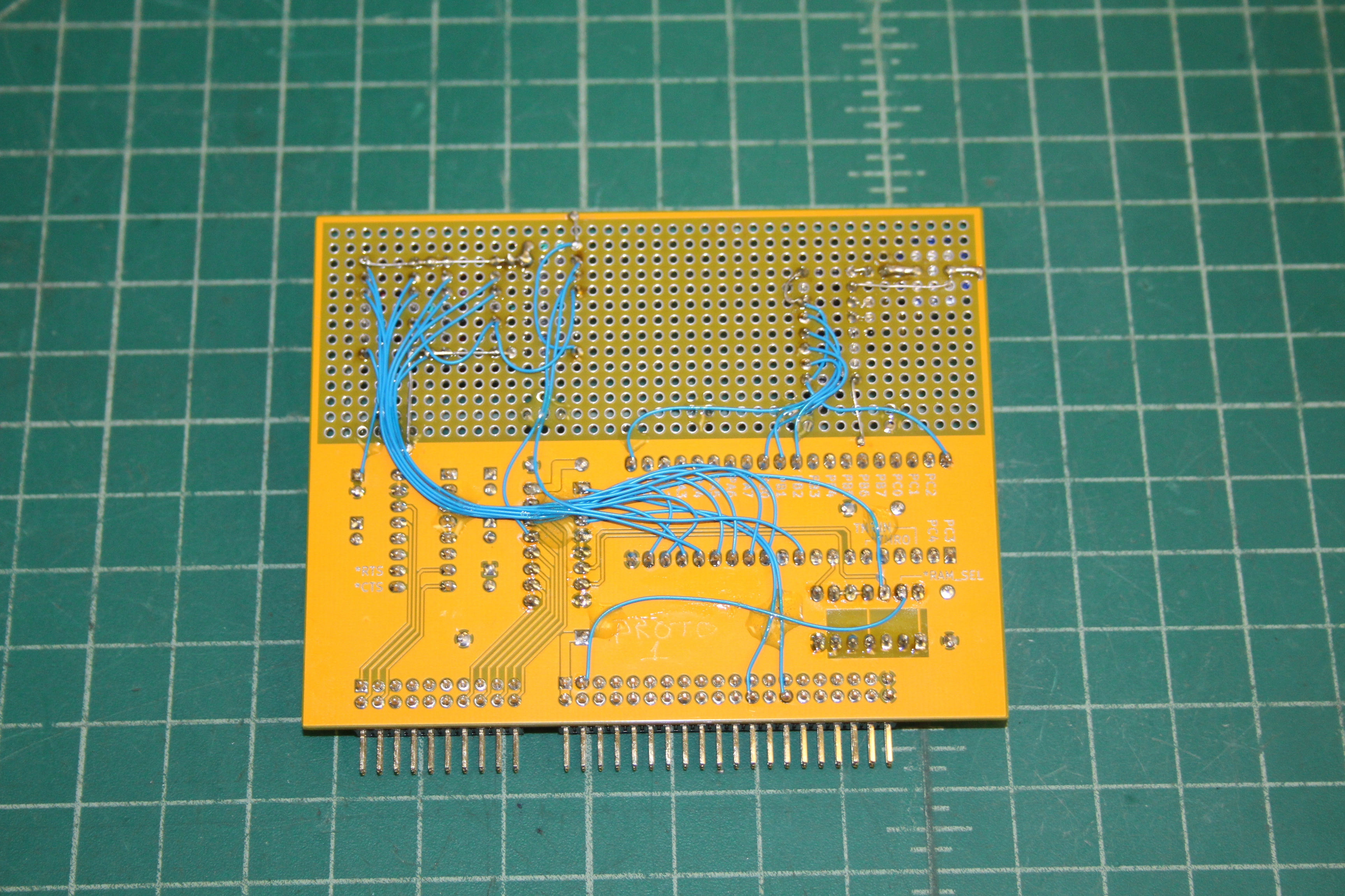
The TIL311s worked fine, and the problem with the Intel 8155 turned out to be a dropped trace for the active-high RESET_OUT line on the backplane! This signal was dropped because I forgot that the expansion connectors would have their rows swapped on the backplane vs. the 8085 SBC rev 1 and expansion cards (this is why Glitchbus boards mount the right-angle connector on the solder side of the board). With the RESET_OUT line brought from the SBC to the SYSINT2 slot with a blue wire, all was well. Here’s a picture of the board running, with 0x44 on the TIL311s:
I exercised the Intel 8155 by interfacing it with a Dallas/Maxim/Analog Devices DS1306 serial RTC. I want to interface a DS1306 to the Certek SBC85-2 boards, but the Certek boards only have 256 bytes of RAM, so it’s difficult to load test programs into memory over serial. The 8085 SBC rev 1 has 8K of RAM onboard, which is plenty for development, and avoids a lot of EPROM burning and erasing.
The DS1306 connects to some of the parallel I/O bits and is very easy to talk to. Aside from the RTC itself, there’s a small supercap and a 32.768 kHz crystal. The DS1306 can be programmed to charge supercaps and/or rechargeable batteries, or charging can be disabled for use with primary cells. There’s 96 bytes of NVRAM available, too. The RTC can also generate 1 Hz and 32.768 kHz outputs and alarm interrupts.
I wrote a small program to enable the charging circuit, clear the DS1306’s NVRAM, set the time, and store a few test values in the NVRAM. I then wrote another program to read the time, format it for display on the serial console, and also display the seconds on the two TIL311 displays. Here’s a screenshot of the clock program running:
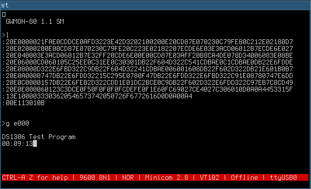
The test program backspaces over the existing time display and overwrites it. Currently, it polls the DS1306 for the time and checks for a change, only writing updates when the value actually differs from the previous display.
Second Prototype
With prototype #1 fixed up and working, it was time to modify it and run a second prototype PCB:
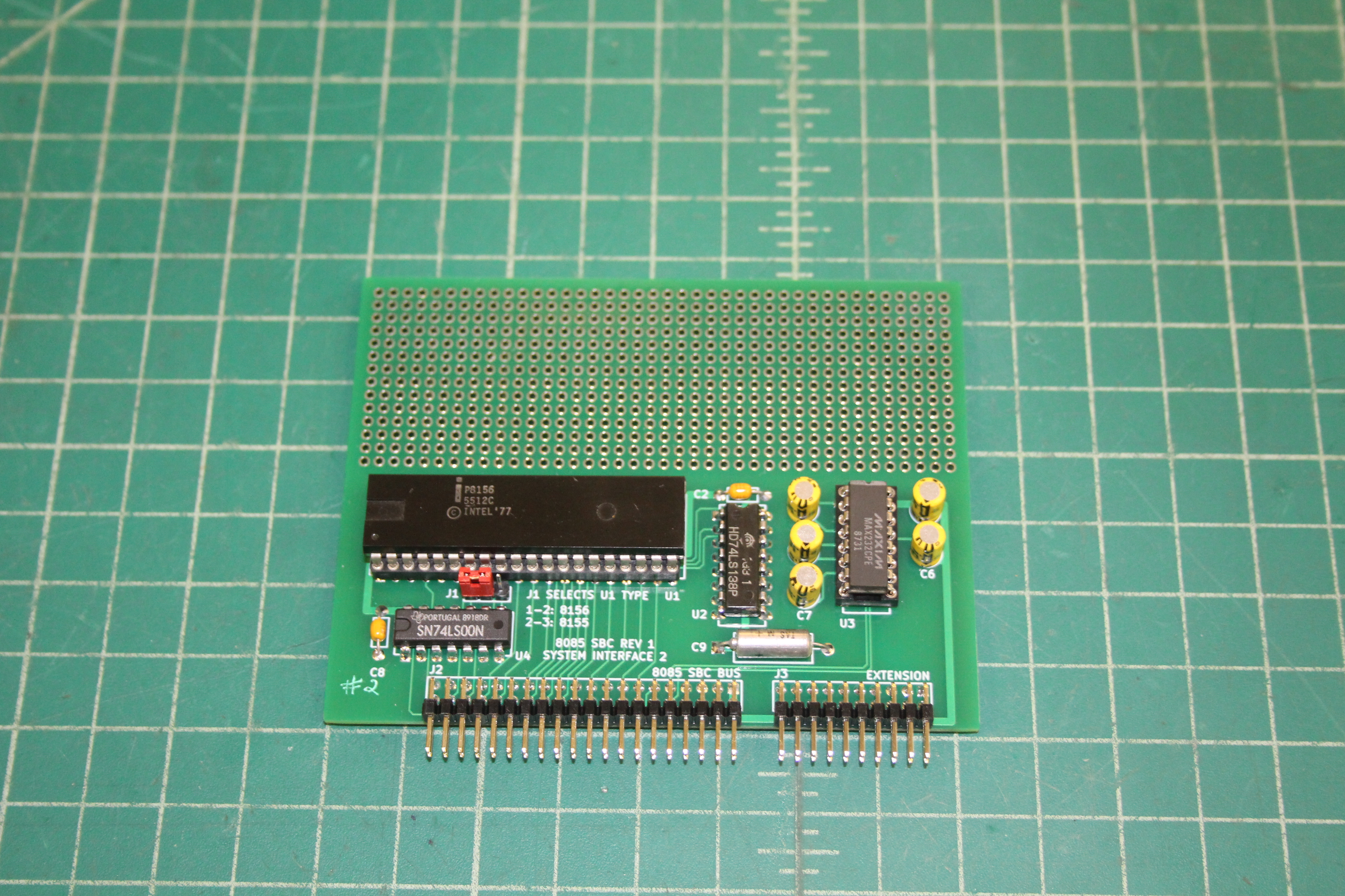
Unsurprisingly, this one works fine. Aside from the ECO related fixes, I also adapted the board for use with either the Intel 8155 or 8156. The only difference between the two chips is that the 8155 has an active-low chip enable, while the 8156 is active-high. This was easily accomplished with a spare section from the 74LS00 quad two-input NAND and a three-position jumper block. This revision also adds the text PROTOTYPE 2 to the bottom of the board, so that it’s easy to identify the revision.
I/O lines toggled