Topic: Certek SBC85-2 cleanup and testing
Date: 2023 MAR 21
I recently picked up a pair of boards from one of the equipment resellers we use. They’re Certek SBC85-2 control computers, and are a very basic Intel 8085 system:
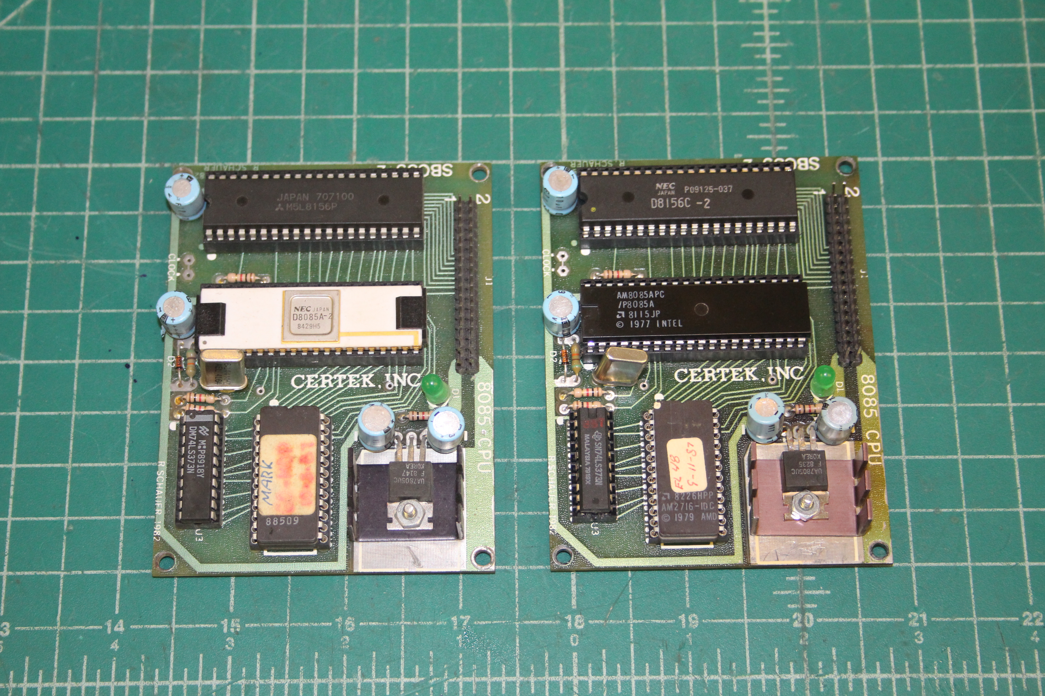
The SBC85-2 contains:
- Intel 8085 CPU with 6.144 MHz crystal
- Intel 8156 RAM, I/O, and timer chip
- 2716-type 2K x 8 EPROM
- 74LS373 latch
- Simple power-on reset circuit
- 7805 regulator and heatsink
- Green power indicator LED
These simple little boards appear to have controlled something to do with a laser system, judging by strings found in their ROMs. They are dated 1982, and were designed by R. Schauer. The names R. Schauer and M. Jimenez were both found in the ROM strings. I’ve been unable to find more information on Certek or what these boards might have been used in. Let me know if you have more information!
Reverse Engineering and Cleanup
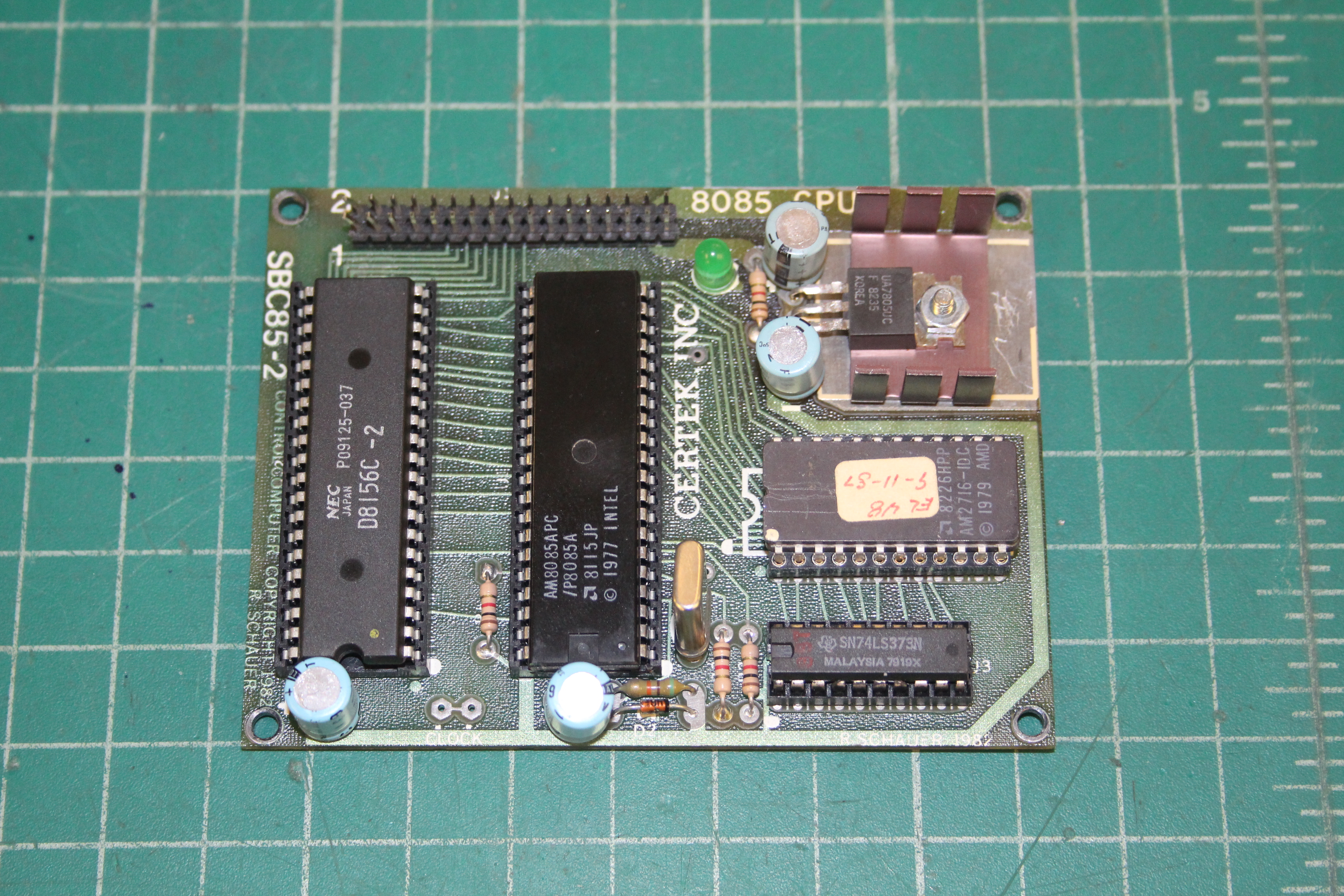
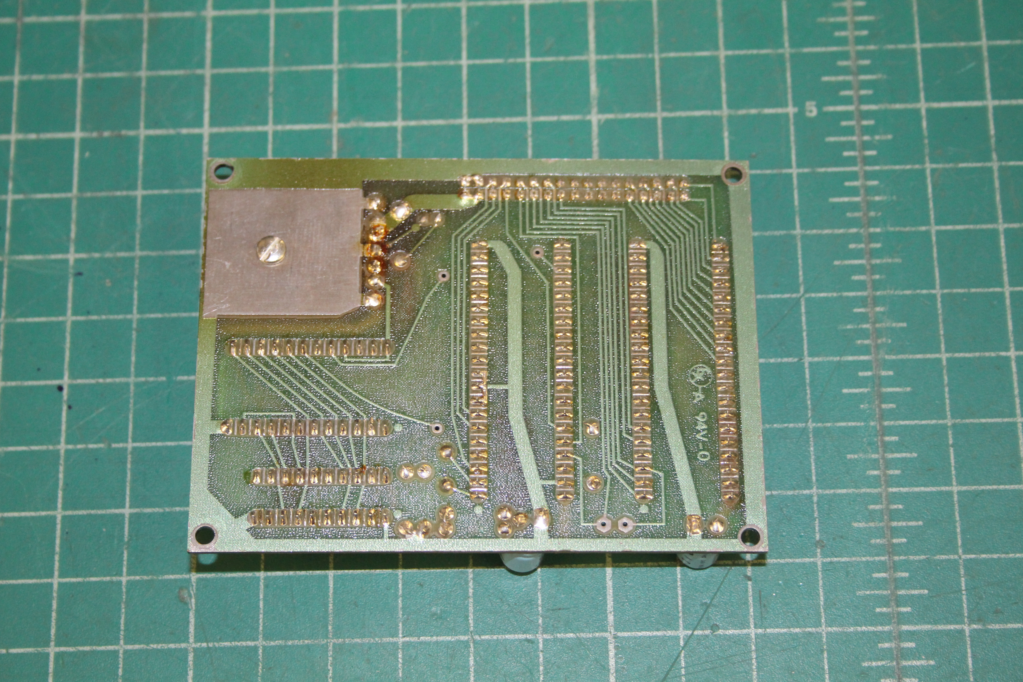
I decided to strip down the board with the plastic 8085 (on the right in the above picture) for reverse engineering and general clean-up since this one appeared to have seen more use than the other. It had heat discoloration in the regulator area, bent pins on its application header, a heavily tarnished 74LS373, etc. Here are some top and bottom shots before stripping:
All of the components were removed with one of our Hakko 472D vacuum desoldering stations. The bare board was cleaned first with denatured alcohol to remove rosin flux, then with hot soapy water. After drying, it was scanned at 600 DPI (contact us if you need the scans).
During clean-up, I found one of the pins on the 8156 was bent up and not making great contact with its socket. I wouldn’t be surprised if the board was pulled from service over that! The pin was straightened and didn’t break.
With all of the components removed, reverse engineering was very easy – not that it’s a complicated board to start with! Tracing the application header was much easier, though. Here’s an ASCII art describing the connector and device mapping:
  Application Connector J1 Pinout
  ===============================

  Pin 1 is furthest from the 5V regulator, on the side closest to the
  Intel 8156.

          SIGNAL   #     #   SIGNAL
      ---------------------------------
             PA1   1 o o 2   PA0
             PA3   3 o o 4   PA2
             PA5   5 o o 6   PA4
             PA7   7 o o 8   PA6
             PB1   9 o o 10  PB0
             PB3  11 o o 12  PB2
             PB5  13 o o 14  PB4
             PB7  15 o o 16  PB6
             PC1  17 o o 18  PC0
      *TIMER OUT  19 o o 20  PC2
        TIMER IN  21 o o 22  PC5
             PC3  23 o o 24  PC4
       *RESET IN  25 o o 26  CPU CLOCK
           READY  27 o o 28  RST7.5
            TRAP  29 o o 30  RESET OUT
             VIN  31 o o 32  GND
             VIN  33 o o 34  GND

  Signals with * in front are active-low.

  TIMER IN and CPU CLOCK are connected together on the board, at a jumper
  area labeled CLOCK.

  VIN is the input to a 7805 regulator, and can be 7.5V to around 12V.


  2716 EPROM
  ==========

  8085 *RD to *CE
  8085 A11 to *OE

  Addressed at 0x0000 - 0x07FF

  Beware, the EPROM can respond to I/O addresses!

  8156 RIOT
  =========

  8085 A12 to CE

  8156 I/O at 0x10 - 0x15
  8156 RAM 0x1000 - 0x10FF
There’s no decoding other than using some of the upper address lines to select between the EPROM and the 8156, so you end up with interesting things like the EPROM responding to I/O reads and the possibility for address conflicts! Probably best not to trip over those scenarios.
This configuration is similar to the three-chip microcomputer schematic found in the MCS-85 handbook, but substitutes the 2716 EPROM and 74LS373 latch for the Intel 8755A (a ROM and I/O chip). A cleaner decode solution would’ve been to use the same upper address line as the chip enable for both the EPROM and the 8156: since the 8156 has an active-high CE, and the EPROM has an active-low *CE, they couldn’t be selected at the same time.
I did cut the connection between *TIMER IN and the CPU’s clock output during cleanup. Both of these signals are available on the application connector, and can be reconnected either on whatever plugs into the application connector, or through the use of a jumper on the SBC85-2 itself.
Reassembly
With the reverse-engineering done, it was time to reassemble the SBC85-2. I took the opportunity to improve the condition of the board, as seen below:
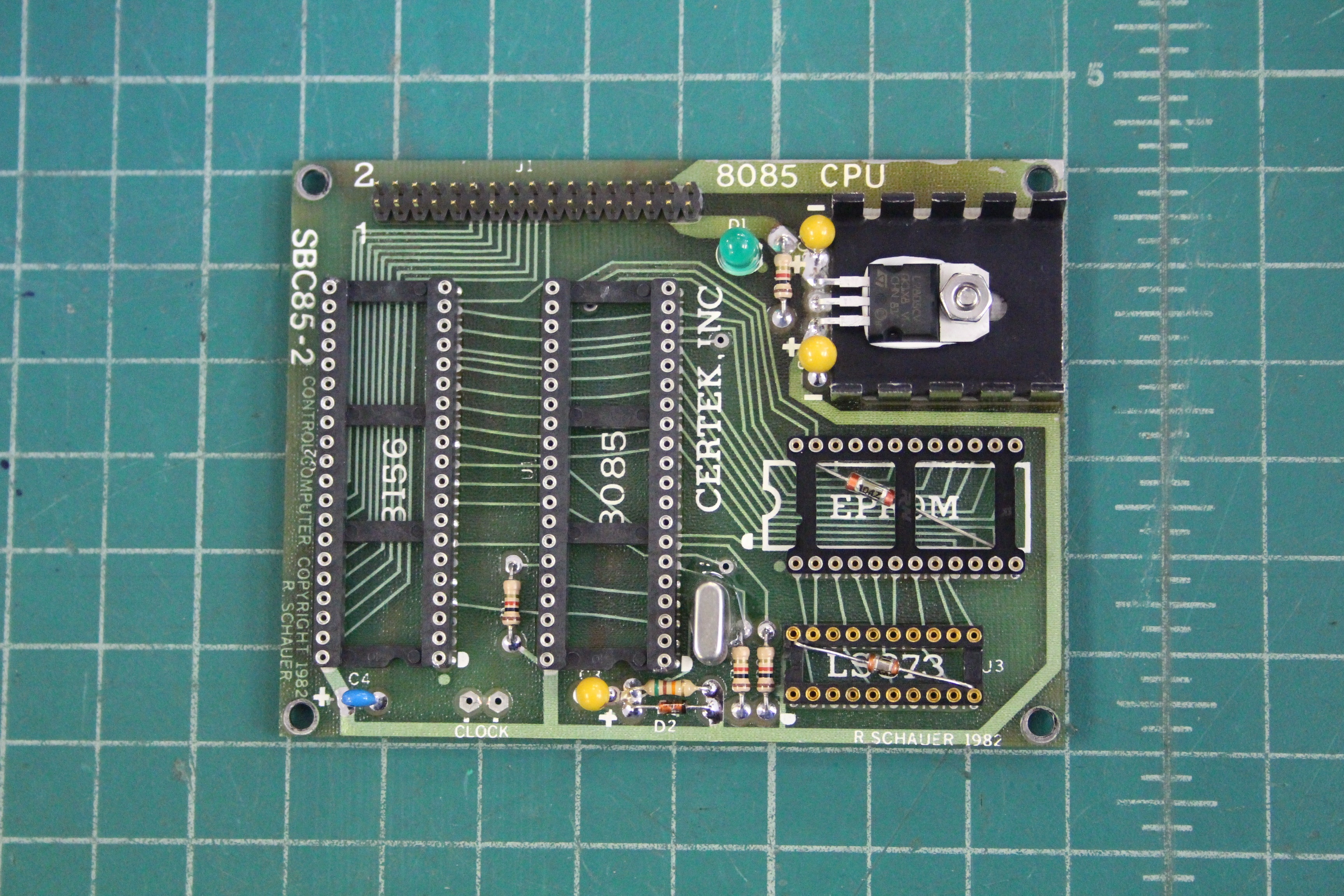
The old single-wipe sockets were replaced with high quality machine pin sockets. The machine pin EPROM socket was also replaced, as the EPROM and the 74LS373 got sockets with integral bypass capacitors. The electrolytic capacitor near the 8156 was replaced with a ceramic 0.1 uF radial capacitor.
The regulator area was improved with a larger heatsink, new 1.5A regulator, and tantalum capacitors. The original heatsink showed signs of having run hot – faded color anodizing, darkened board substrate, and darkened/flaking solder mask. I suspect the smaller heatsink that the board came with was installed due to clearance issues with the regulator legs. Our standard Aavid/Thermalloy single-hole heatsink hit the regulator’s legs when installed with a #4-40 screw, so a heatsink with a “slop slot” (the top end of which can be seen above the regulator tab) was used instead. This allowed enough clearance between the heatsink and regulator legs, and will provide much better cooling.
The reset circuit’s electrolytic was replaced with a 10 uF tantalum capacitor, as the electrolytic was kind of crammed in there. A new application header was installed, since the original had several bent pins that broke during straightening. The 6.144 MHz crystal was secured with a dab of two-part epoxy.
Testing with GWMON-80
To test the board, I customized GWMON-80 for the SBC85-2 using the 8085 bit-bang serial driver I’d recently written. The 8085 has built-in hardware to assist with bit-banging, and its use is covered in Intel application note AP-29, from which the routines in the GWMON-80 are largely derived.
The 8085 SID and SOD lines don’t go anywhere on the SBC85-2, so they were connected to using minigrabbers:
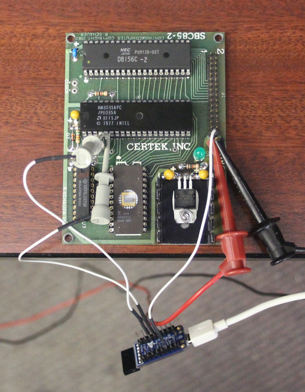
While even hardware assisted bit-bang serial isn’t as good as a real UART, it certainly makes testing boards like the SBC85-2 easy! SID and SOD are TTL level lines, which means they can be connected directly to a USB to 5V serial interface, like the Adafruit CP2104 Friend seen above.
The SBC85-2 wants unregulated input power, meaning I couldn’t just power it from USB. +8V was supplied from one of our Harrison 865C adjustable bench supplies:
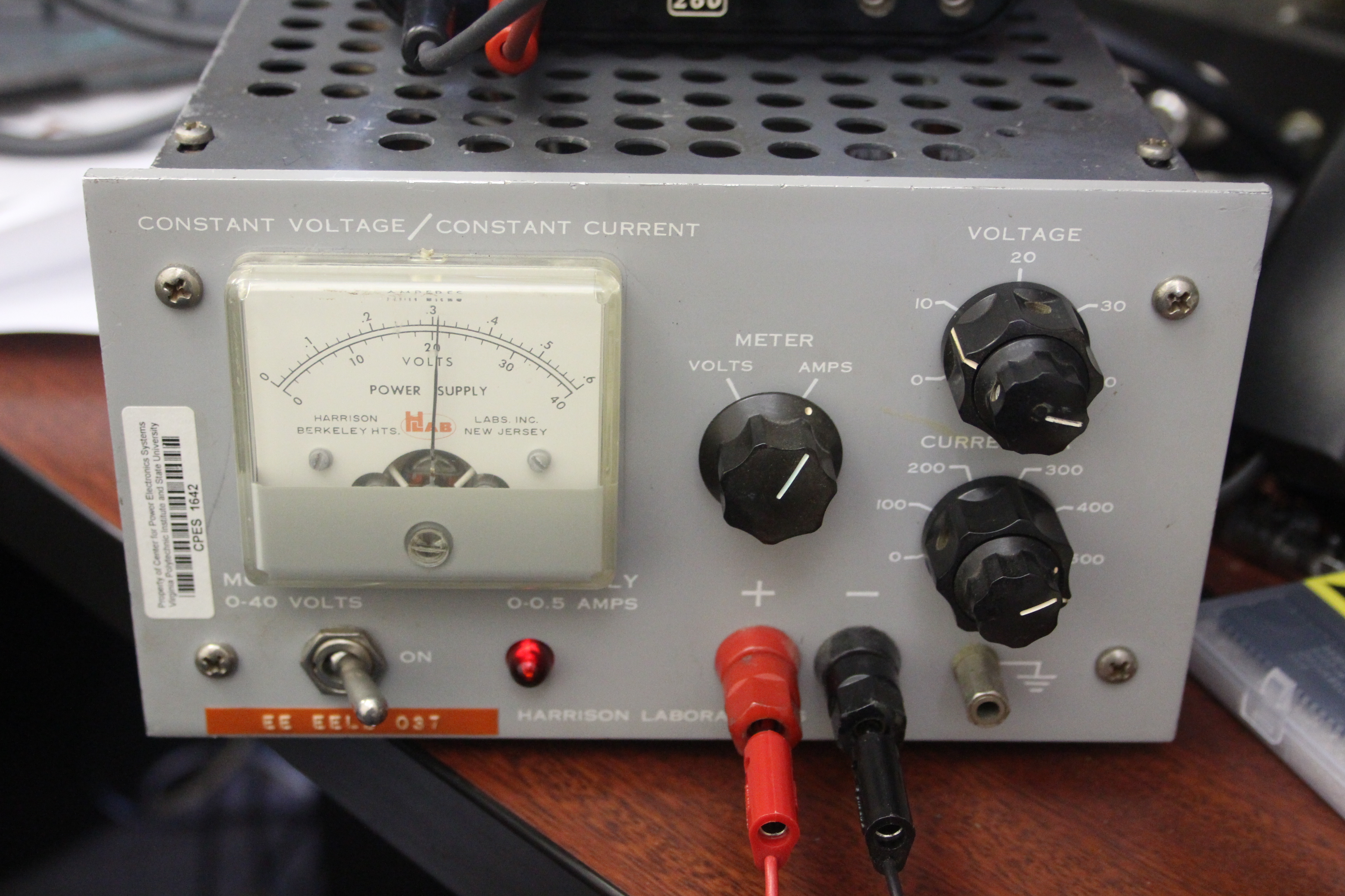
It draws a bit of power, for such a simple board! GWMON-80 came up – there’s no reset button on the SBC85-2 itself, so if you need to reset, power-cycling is the easiest way, though *RESET IN is present on the application connector. Using GWMON-80, I was able to read the 8156 I/O ports, then set the command register to change the ports from inputs to outputs. Writing values to the output ports was checked for a few pins and worked fine!
industrial 8085 boards running