Topic: Cleaning up the 8085 SBC rev 1 for a project
Date: 2023 JUL 19
My first single-board computer PCB design was the original 8085 SBC rev 1 board from 2010. This board was designed in EAGLE CAD and manufactured back in the dark times, when a single 4x3 inch board cost $40, came with no solder mask or silkscreen, and took months to arrive. I still have the board, of course! It’s been used for a number of experiments and tests, but was never committed to anything permanent, and was usually floating around the shop.
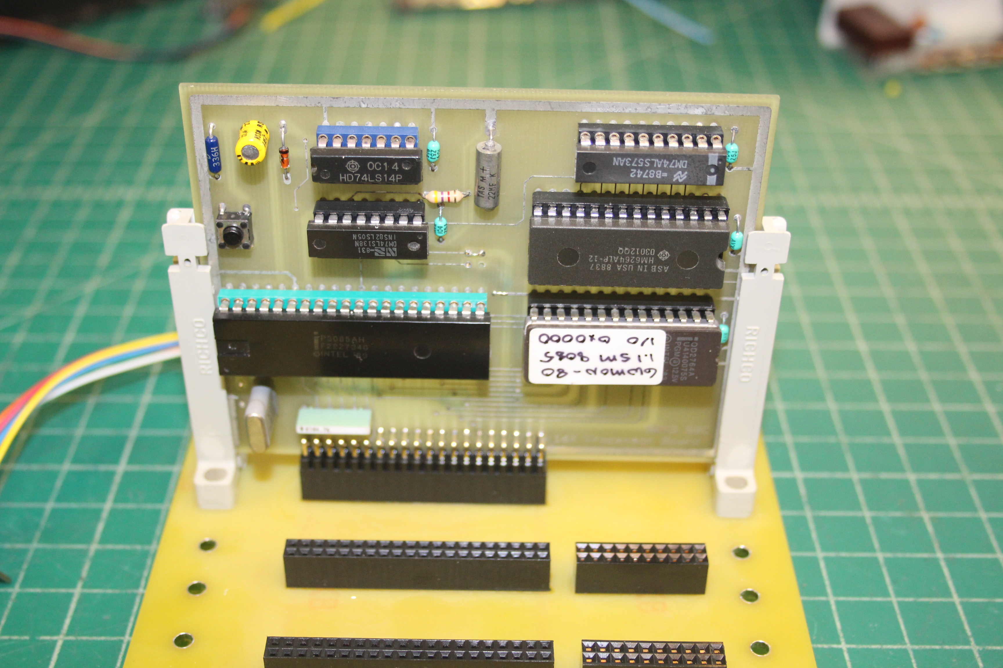
A few months ago, I decided to start a new project that would include an 8085 processor, and thought it’d be a good excuse to clean up the 8085 SBC rev 1 and give it a permanent home. There were a few things that needed fixed: the original resistor pack was cracked, some parts had been stolen from their sockets, and the board was just generally dirty. It got a general cleanup:
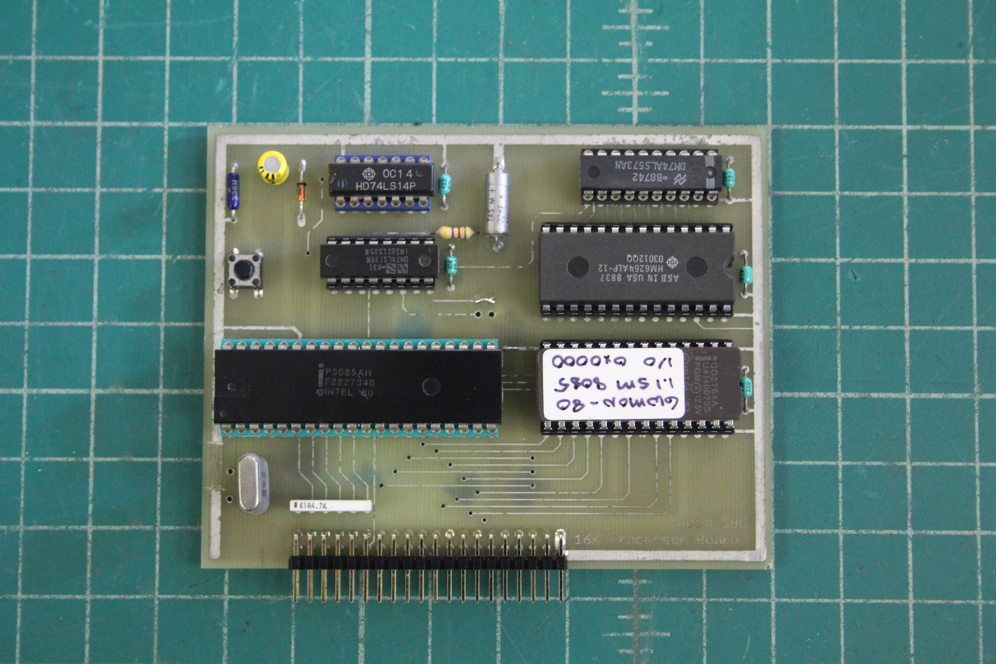
The electroless tin surface finish has not aged well, and often required a little cleaning with an ink eraser before it’d solder properly. It’s very thin, and often went straight to copper if there was any significant tarnishing. The following items were replaced:
- Pull-up resistor pack, 4K7, 5 element bussed
- Missing 6264 8K x 8 SRAM replaced
- Missing CPU replaced with Intel 8085AH
- Missing logic chips replaced
- Expansion bus connector replaced with right-angle header
- Crystal changed to 6.144 MHz for bit-bang serial
The ROM installed when clean-up started contained some test program for a forgotten project. I decided to customize GWMON-80 using the 8085 SID/SOD bit-bang serial routine I’d written, which would allow the 8085 SBC rev 1 to talk serial despite lacking a dedicated UART. This will be good enough for its intended use.
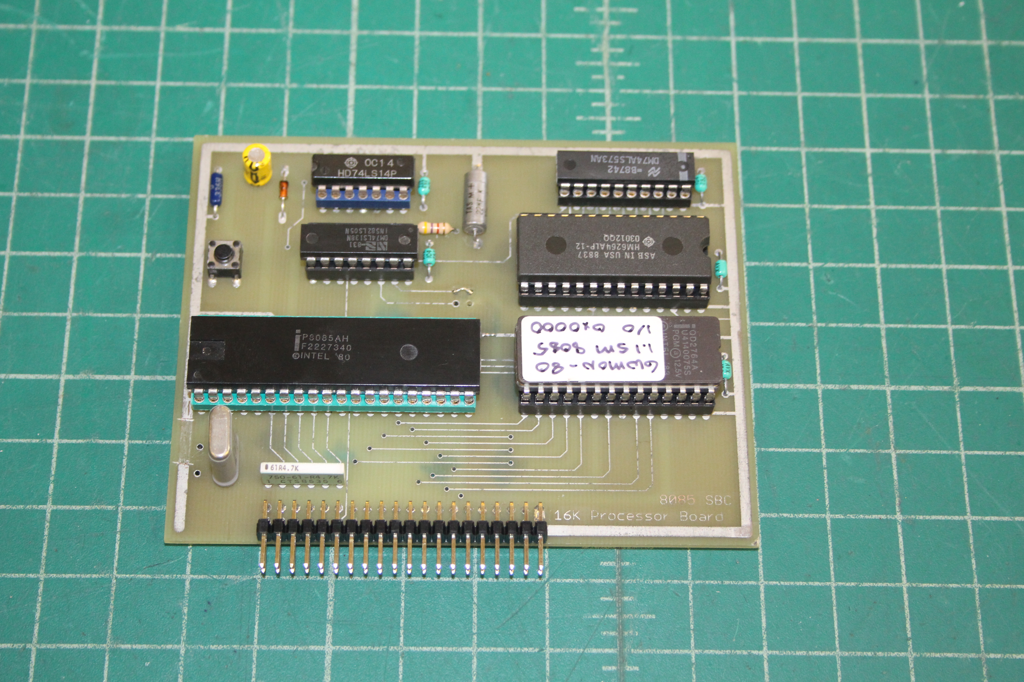
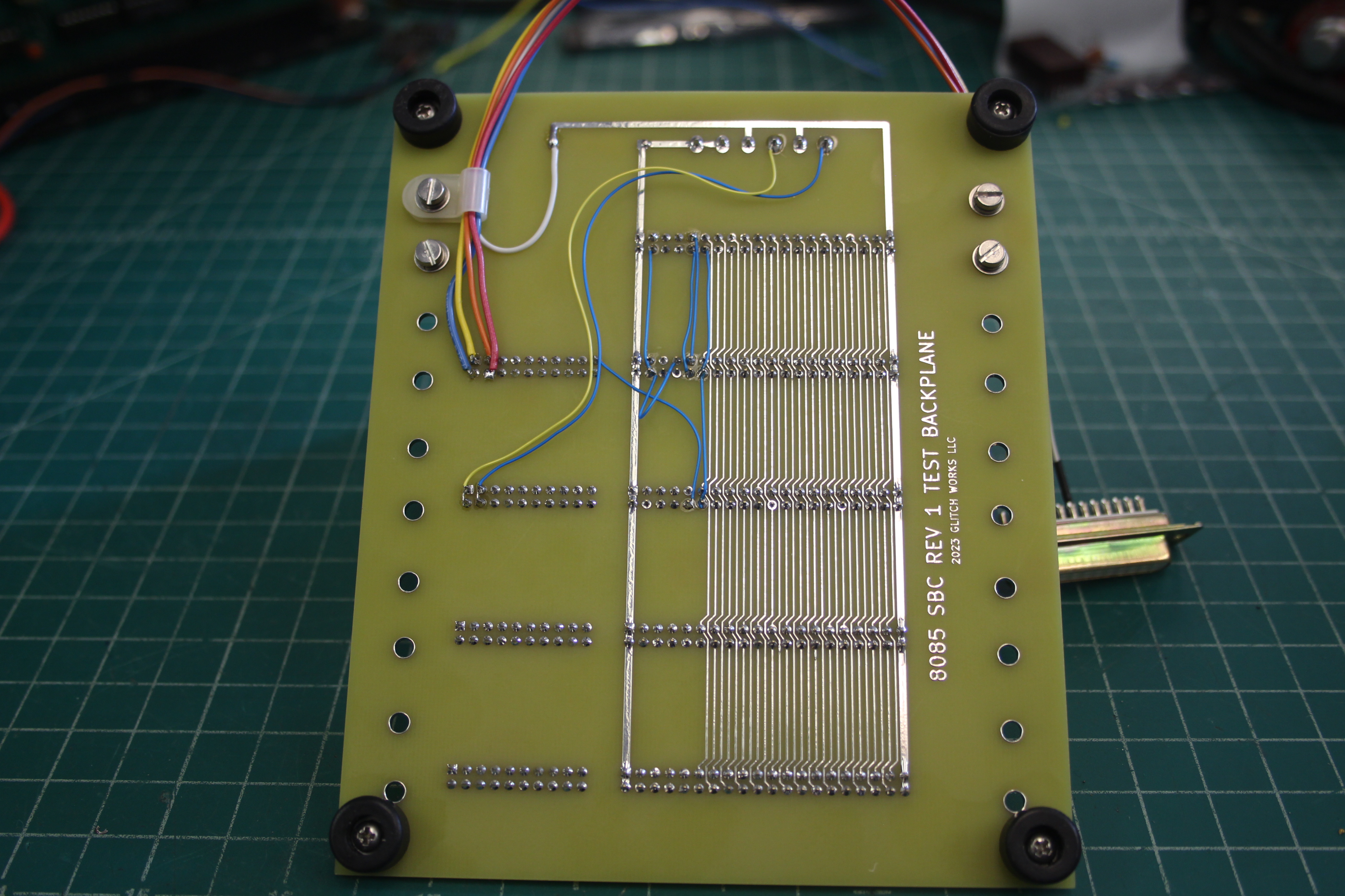
The clock crystal required some modification:
To the left of the crystal can be seen an old modification: the +5V power trace has been cut and scraped back to prevent shorting to the crystal case. I think I’d shorted +5V to something else due to that once, and decided to cut it! The crystal is also now rotated, as it was too close to the edge of the board for the intended application. This modification required removing the oscillator capacitor, cutting a trace, and running a wire on the back. There are quite a few blue wires, now:
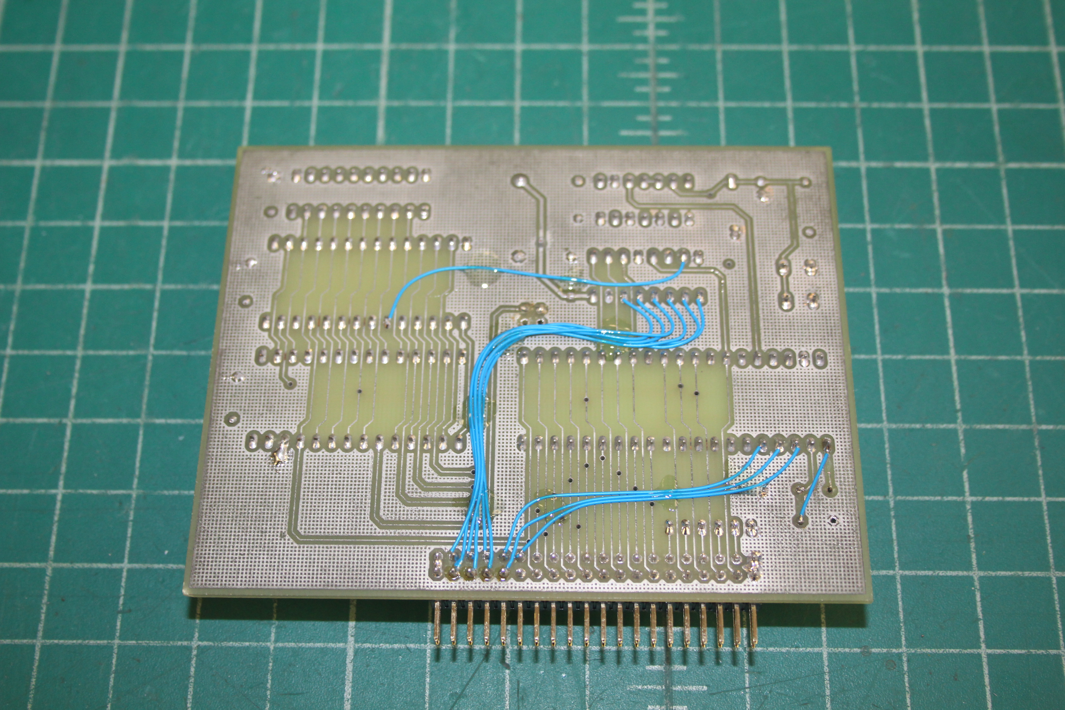
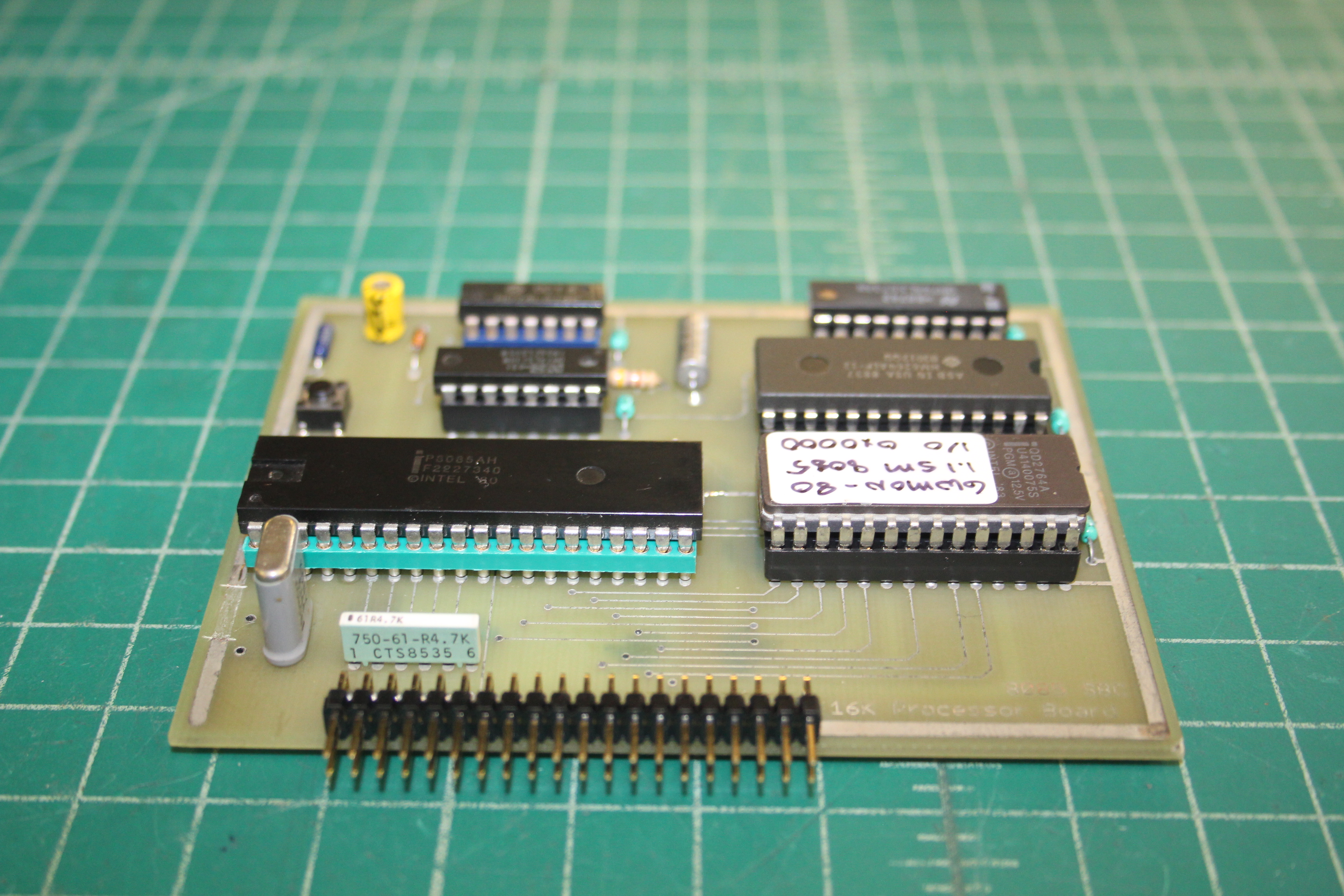
The blue wire running from the 74LS138 to the SRAM readdresses the SRAM to 0xE000 - 0xFFFF, so that the same software can be run on both this board and the 8085 SBC rev 2 board. This change was done a while ago.
Below that, there are now six blue wires running down to the expansion connector from the 74LS138. These allow boards on the expansion bus to use the onboard memory decoding, and will simplify the design of other boards. These lines are all active-low chip selects.
There are three blue wires running from the 8085 to the expansion connector. One of these connects to the RESET output of the 8085, which is active-high and used by a bunch of the MCS-85 family chips. This was run to pin 4 for the scrolling LED display, but now lands on pin 11 so it’ll match the revision 2 boards.
The remaining two wires from the 8085 carry SID and SOD so that they can be used for bit-bang serial I/O. These can be picked off with DuPont connectors or minigrabbers for TTL serial, or be level shifted on another board.
I decided to go with the right-angle header and a backplane due to the lack of mounting holes in the 8085 SBC rev 1 board. Holes were added in the second revision, which permits PC/104 style stacking. The right-angle mounting will actually work out better for the intended application, anyway. For ease of testing, I laid out a test backplane for development and experimentation:
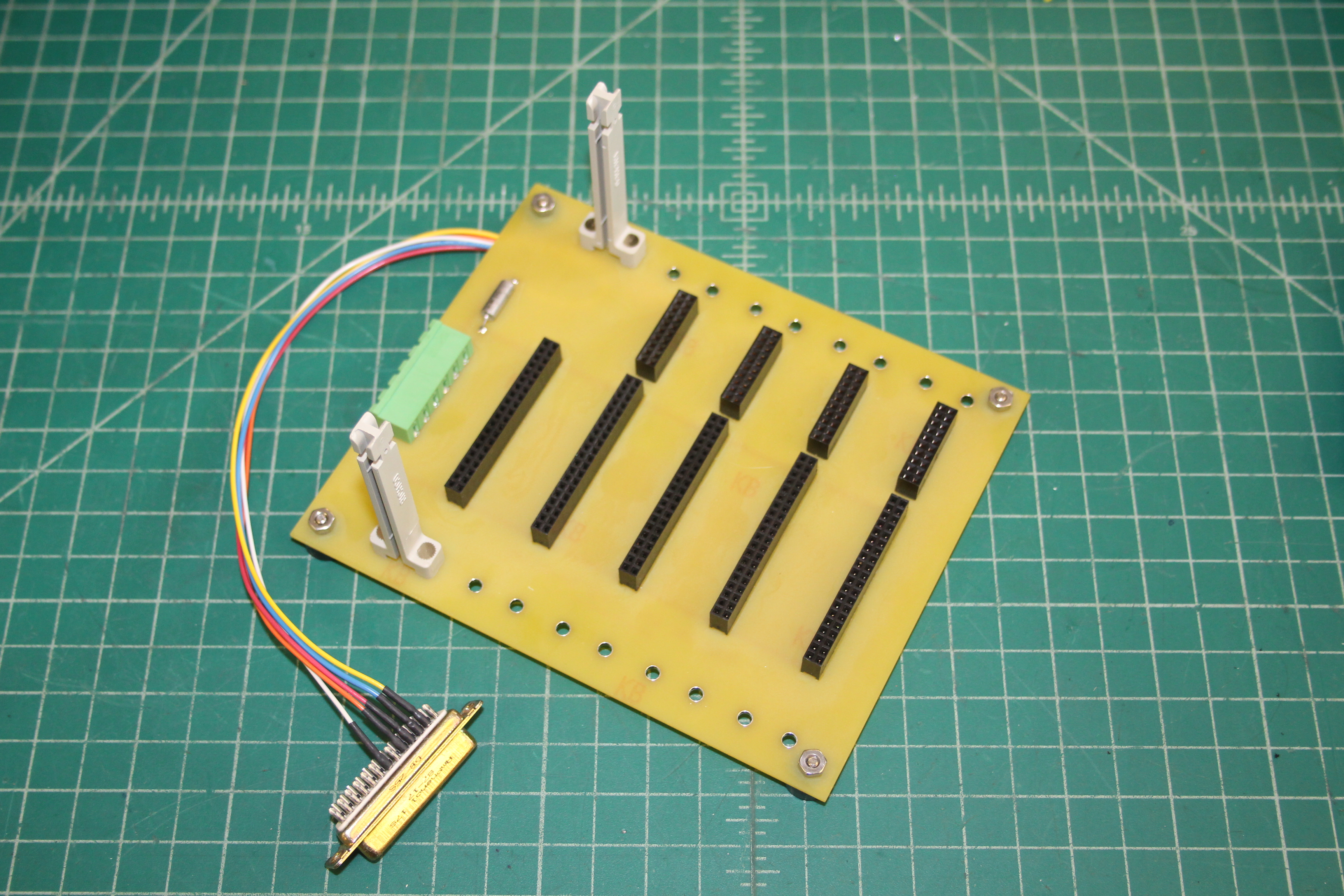
The above image shows why the crystal had to be moved: it would’ve interfered with the Richco card guides. I had a bunch of these laying around from a previous work project, and decided to use them here. I removed the board locking mechanism since there’s no corresponding locking hole in the 8085 SBC rev 1.
There’s also an additional connector on the backplane for the slots other than the CPU. This will allow for I/O through the bottom edge of the card, which is again something the final application will require. The bottom of the backplane busses only the dedicated signals on the 8085 SBC rev 1:
The idea here is that the uncommitted pins on both the 40-pin expansion connector and the 20-pin “extension” connector can be used for whatever purpose necessary using flywires. There was one goof-up on the backplane: the RESET_OUT signal was not properly routed. I forgot that the connectors on the backplane would be reversed from the 8085 SBC rev 1! The routed line would be *MASK on the 8085 SBC rev 2, but is unused on the rev 1 boards.
There’s obviously some work already done on the backplane: a pigtail to a DB25F can be seen running to the first non-CPU slot, as well as some address select and other wiring. Those bits will be covered in a future writeup!
old projects repurposed