Topic: Building an OSI 400 and testing CPUs
Date: 2022 SEP 16
Quick Links
- PDF copy of the OSI 400 manual, thanks to Dave’s OSIweb
- Reproduction OSI 400 Boards and Parts Kits
- Relevant ROM images, via HTTP
- Relevant ROM images, via FTP
Ohio Scientific 400 Superboard Build
In October 2021, a friend brought several interesting processors to the shop for testing. Rather than just use something already running, I decided to build up an original blank Ohio Scientific 400 “Superboard” I had on hand. This board had already been scanned, and reproductions made available. I’d gone through a copy of the manual beforehand and set aside enough parts to finish the build. The build pretty much followed the manual, and my OSI 400 was configured for the Motorola 6800:

As seen above, the board was populated with a mix of old and new components. The large sockets were NOS or solder pull Augat. 16-pin sockets were solder pull EMC from some scrap boards traded to me by Bill Degnan. A NOS socket has been installed for the 555 timer. There are no 14-pin sockets for the 7403 open-collector NAND gates above, but those were eventually populated with NOS Augat sockets.
TangentDelta built a ROM adapter to allow the use of a 28C64B EEPROM in place of a 1702A EPROM (green perfboard with blue wires). This allowed us to run test programs on the processor without burning 1702A EPROMs. At the time, my 1702A programmer(s) were in unknown/nonworking condition. The 28C64B -> 1702A adapter does require a flywire for the ground connection, as the 1702A has no ground pin!
No RS-232 or current loop circuitry was populated at this time, we used a USB to TTL serial cable for initial testing. The 555 timer for the bitrate oscillator was also left out, and a serial clock was run in through the Pomona grab leads from a HP 8116A pulse/function generator, set to 4.8 kHz. This frequency gives a x16 ACIA clock for 300 BPS.
So, why the fuss for a Motorola 6800? Well, the 6800 build was really just so that the board could be confirmed fully functional before testing the processors a friend had brought down…
MOS Technology 6501 CPUs
The actual processors to be tested were some MOS Technology 6501 processors! The OSI 400 setup (400 board, backplane, and my prototype RAM board) was moved to another workbench, along with a HP 6213A power supply, HP 8116A pulse/function generator, and ADM-3A terminal:
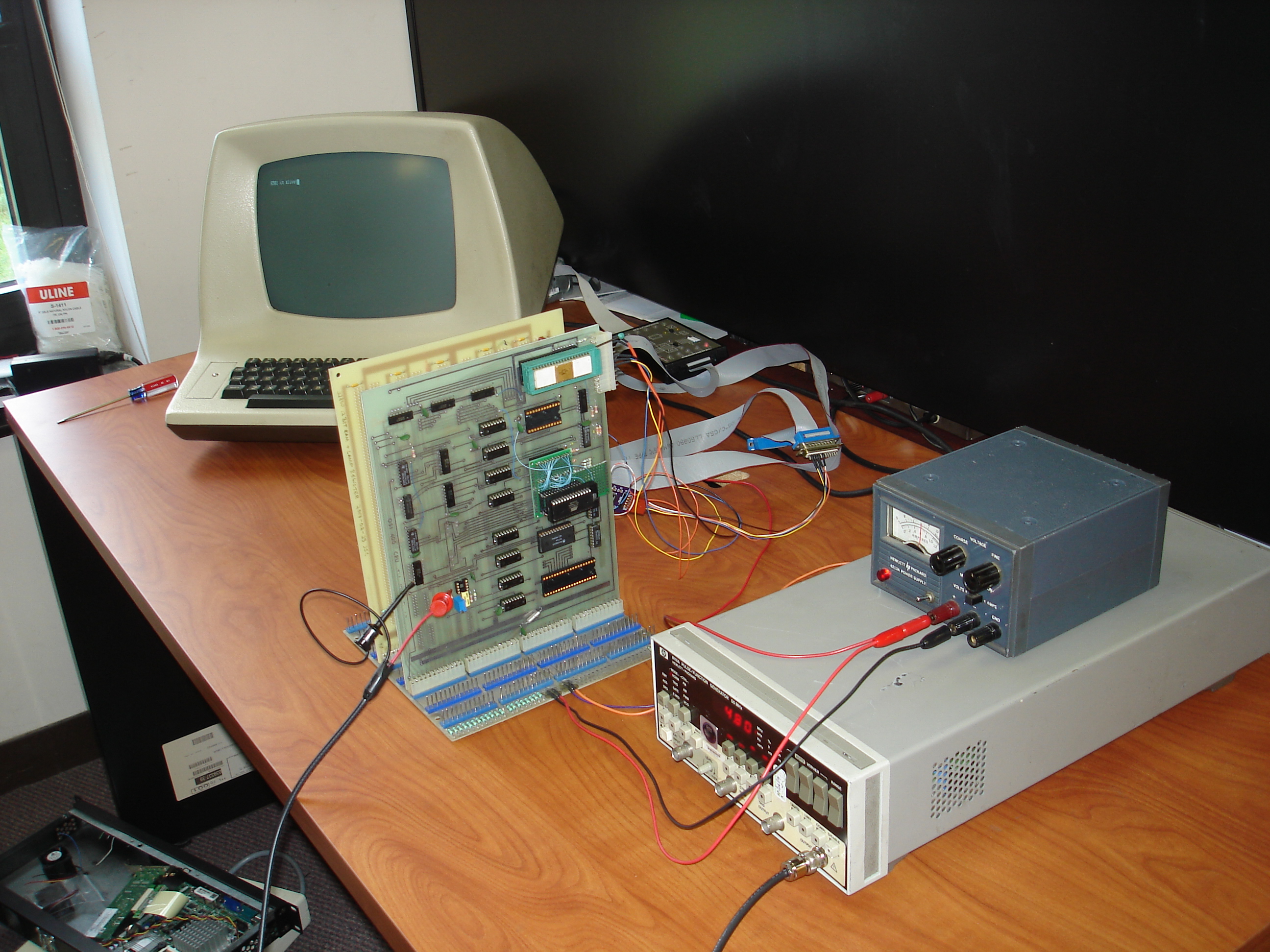
Here’s a closeup of the first MOS 6501 we tested:
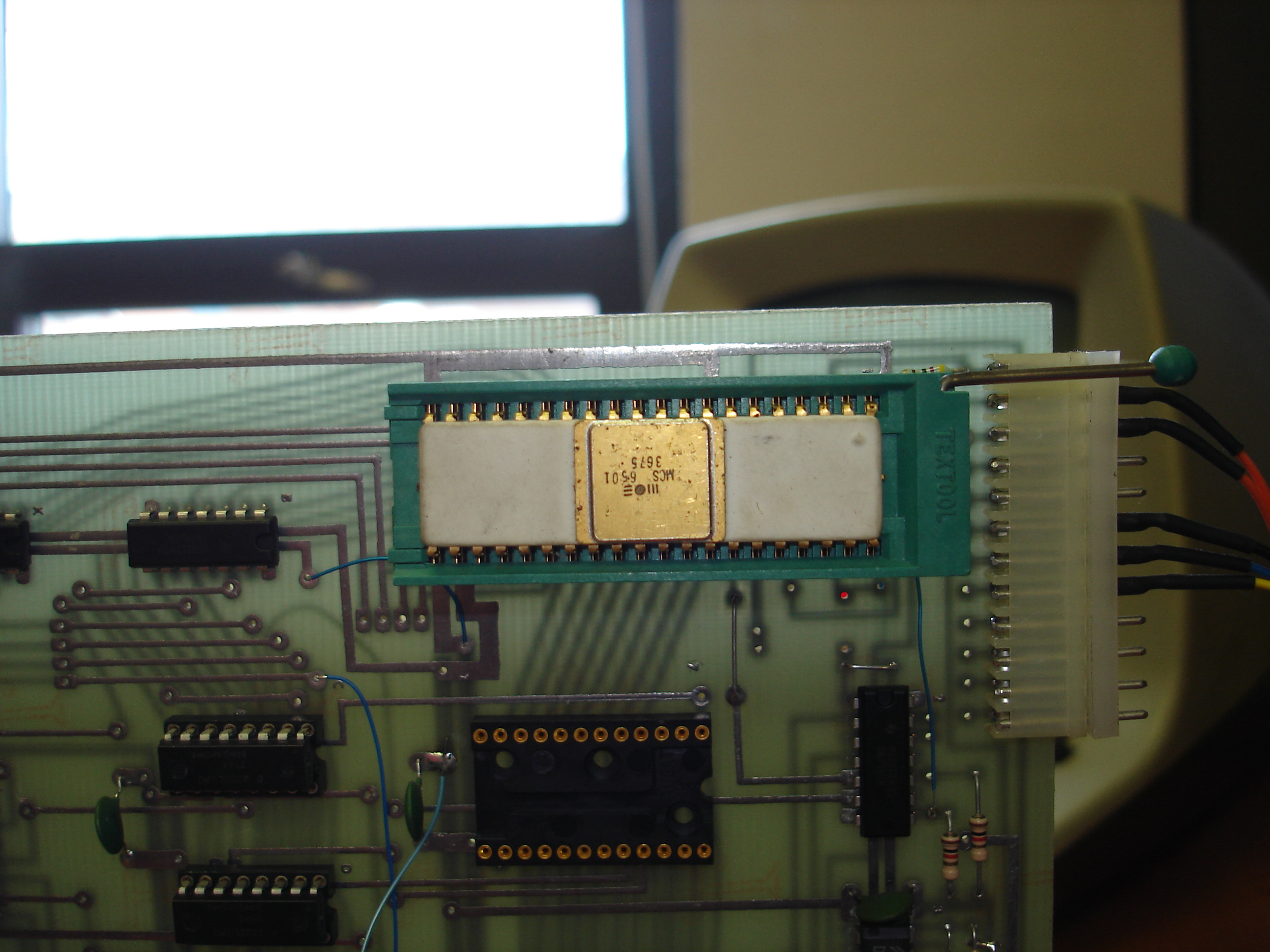
TangentDelta wrote a quick test program to initialize the Motorola 6850 ACIA and print a string. While the program was small and simple, it did not work at first, despite working fine on a 6502-based OSI setup! It turns out we’d tripped over the ROR bug, an issue found in very early MOS 6502s, and apparently in the MOS 6501 as well. With the ROMed program modified to avoid using the ROR instruction, we got output:

This confirmed a few things:
- This particular MOS 6501 was working just fine
- MOS 6501s do have the
RORbug - The Ohio Scientific 400 Superboard really does let one drop in a MOS 6501
We were able to test one of the other MOS 6501s, but the third had too much lead damage for us to make a determination one way or another.
Cleaning up the OSI 400 Superboard
With the required testing done, I set about cleaning up the OSI 400 board and making a few changes:
- Figure out why onboard SRAM was not functional
- Build the RS-232 level shifters from the OSI 400 manual
- Fix the 555-based bitrate oscillator
- Tack down all flywires
- Change out resistors and timing capacitors for vintage components
- Test a Rockwell R6512 CPU as a MOS 6501 substitute
Onboard RAM Problems
The RAM failure turned out to be a dead 7403 open-collector NAND gate. The two 7403s had been desoldered for initial testing after the onboard RAM failed to work with the OSI 68A2 ROM monitor since we had limited time to build and debug the board. These two ICs should always be socketed, mainly because you must remove or disable them to use external RAM with the OSI 400 board in its default configuration. The plastic package 2102 SRAMs were replaced with some ceramic chips:
These chips, and the sockets they’re installed in, were removed from some scrap boards that Bill Degnan had traded me a long time ago. They are house numbered, but are Intel 2102s. They were in very nice EMC machine pin sockets, so the sockets were desoldered and used in this OSI 400 build.
RS-232 Interface and Bitrate Oscillator
The OSI 400 board’s manual includes a schematic for their recommended RS-232 level shifters. These are built with discrete transistors – older copies of the manual may include a circuit made with OP-AMPs, which apparently should be avoided, according to newer copies of the manual. To keep with the “vintage look” build, I found a pair of TO-106 packaged transistors in the parts bin, and built up the level shifters:
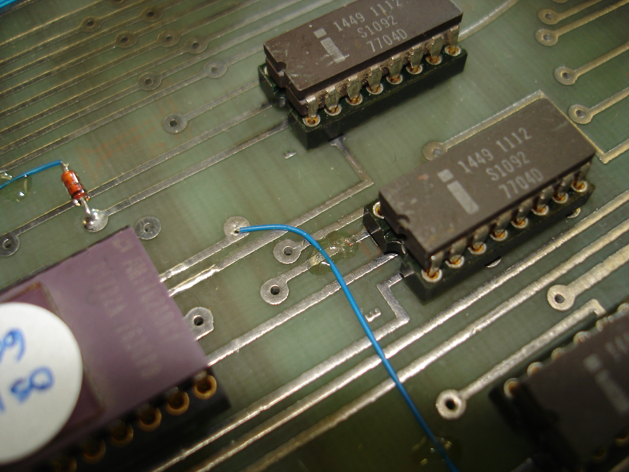
Almost any transistor will work, though a PNP and NPN are required. I probably should’ve built the level shifters on the uncommitted DIP footprint above the location where they’re shown in the above picture, but they don’t hurt anything where they are. I did opt to use uncommitted elements of the 7404 inverter to the left of the RS-232 shifters to buffer them from the 6850 ACIA, as recommended in the manual.
For the bitrate oscillator, don’t forget that an 0.01 uF capacitor is supposed to be tacked onto the back of the board, from the 555’s pin 5 to ground:
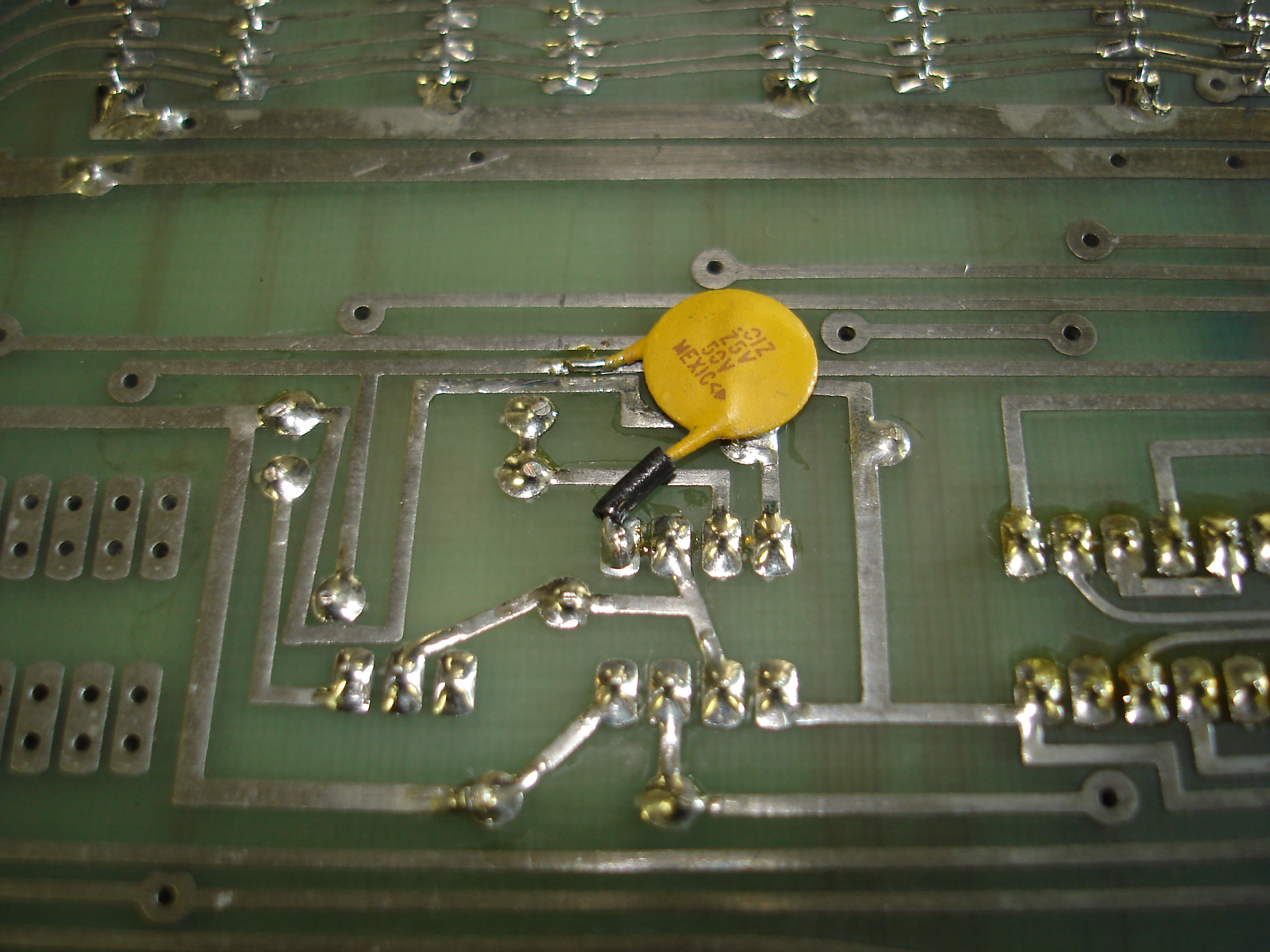
I was unable to get the bitrate oscillator, which is based on a 555 timer, to function correctly above 300 BPS. This was due to suggested resistor and capacitor values from the manual producing a very uneven square wave (duty cycle was nowhere near 50%), and tolerances/thermal coefficients of capacitors and resistors I had on hand. I ended up using 1% metal film resistors, but had to “guess and check” values for the capacitor. The value which gave best adjusting range on the trimmer was 56 pF. Polystyrene capacitors were ordered for the bitrate oscillator, both for their excellent temperature stability and vintage look. Do not use a ceramic capacitor here! Just the heat from placing a finger on the capacitor will cause a frequency drift of several kilohertz with the values required for 9600 BPS operation!
Vintage Components
Since this board was an actual vintage blank (as opposed to a reproduction), and since many of the socketed components were vintage, I decided to replace as many components as possible with vintage parts. For this, I changed all of the standard resistors over to 1/4 W carbon composition types, except for the two critical resistors in the bitrate oscillator. Those two were replaced with NOS 1% mil-spec parts. The board had been built up with ceramic disc capacitors for bypass, and an axial hermetically sealed tantalum for bulk decoupling, so those were no problem.
Timing capacitors were replaced with axial polystyrene capacitors for a couple of reasons. First, and most importantly, polystyrene capacitors have a very low temperature coefficient; that is, their capacitance changed very little with change in temperature. While there are newer capacitor types which have equal or lower tempcos, polystyrene was an excellent choice in the mid to late 1970s, when this board was designed.
The OSI 400 board now looks like this:
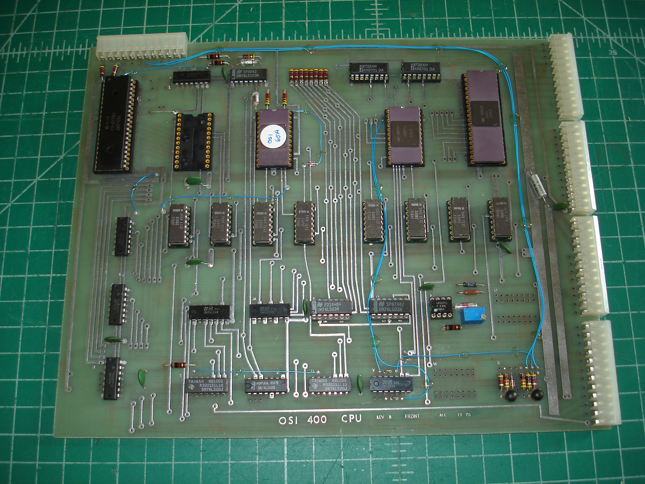
All of the flywires have been tacked down using 5 minute two-part epoxy. We’ve been through a number of brands at the shop, and have settled on Devcon 5 minute epoxy, which ironically used to be about the only thing one could find at the hardware store.
I have a number of AMI second-source ICs from the Motorola 6800 family, acquired from scrap Sundstrand CNC machine circuit boards. Here’s the AMI 6850 ACIA and 6821 PIA installed in their sockets:
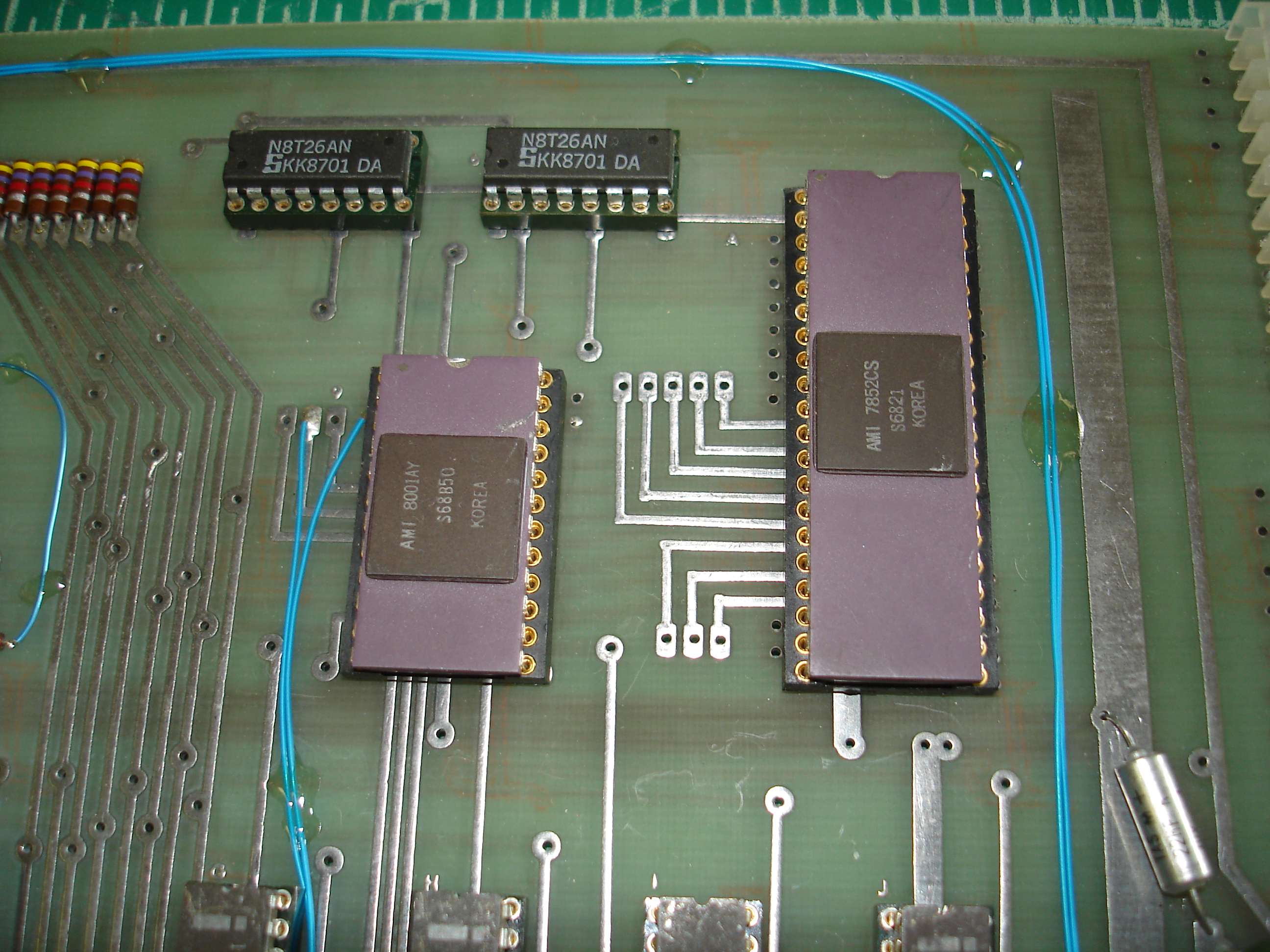
Note that the PIA is not yet wired in. In the above image, the green solder pull EMC 16-pin sockets can be seen under the 8T26 bus transceivers, as can the Mallory TAS-M wet tantalum on the +5V rail.
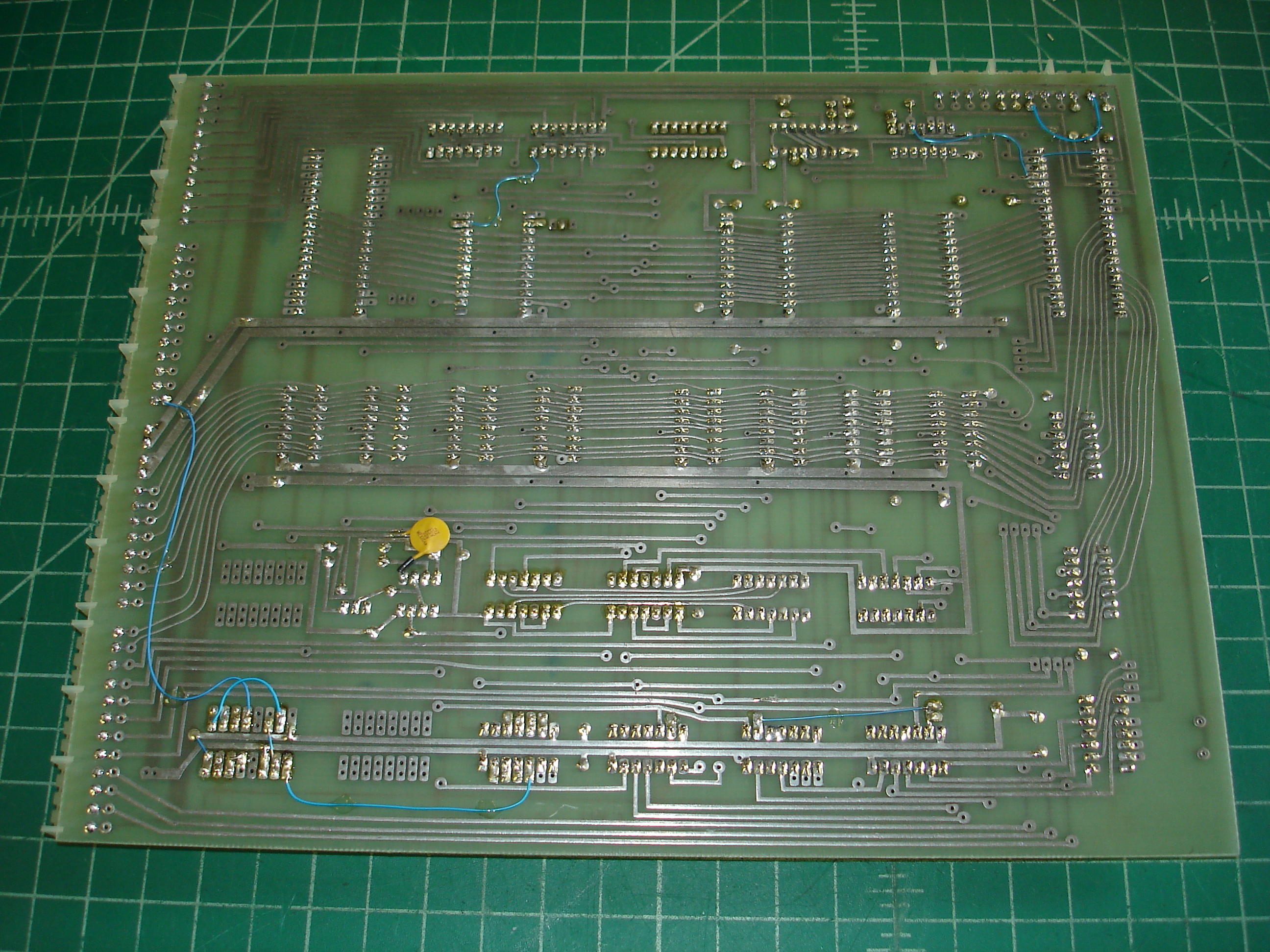
Copies of the OSI 65A monitor (6502 ACIA operation) and 68A2 monitor (6800 ACIA operation) were burned to AMD 1702A EPROMs. These files are available here, via FTP, or here, via HTTP. The 65A ROM will work at either 0xFF00 or 0xFE00 due to the vector table at the end of the ROM. The OSI 400 board decodes both locations to the 1702A in the socket closest to the ACIA.
Note that there’s a critical trace cut just below the 1702A EPROM:
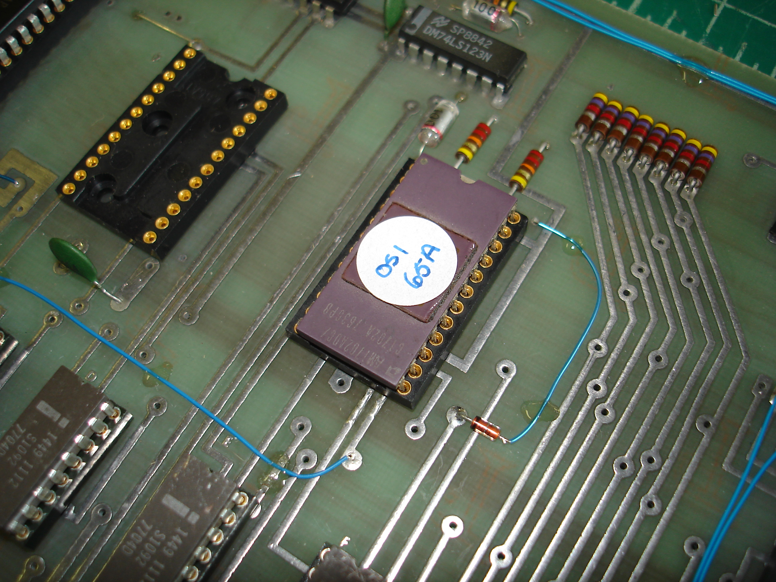
The trace cut shown is critical to the operation of the OSI 400 board, if using onboard EPROM. Without this cut, the EPROM will never select! This caused some quantity of frustration when getting the OSI 400 up and running for the first time.
Rockwell R6512 Processors and the OSI 400
The Rockwell R6512 is an interesting 6502 variant: it requires a two-phase clock, like the Motorola 6800 and MOS 6501. It also has a DBE (Data Bus Enable) pin, though it lacks the MOS 6501’s TSC (TriState Control) pin. I wanted to try the R6512 in the OSI 400, with the 400 board still configured for the MOS 6501:
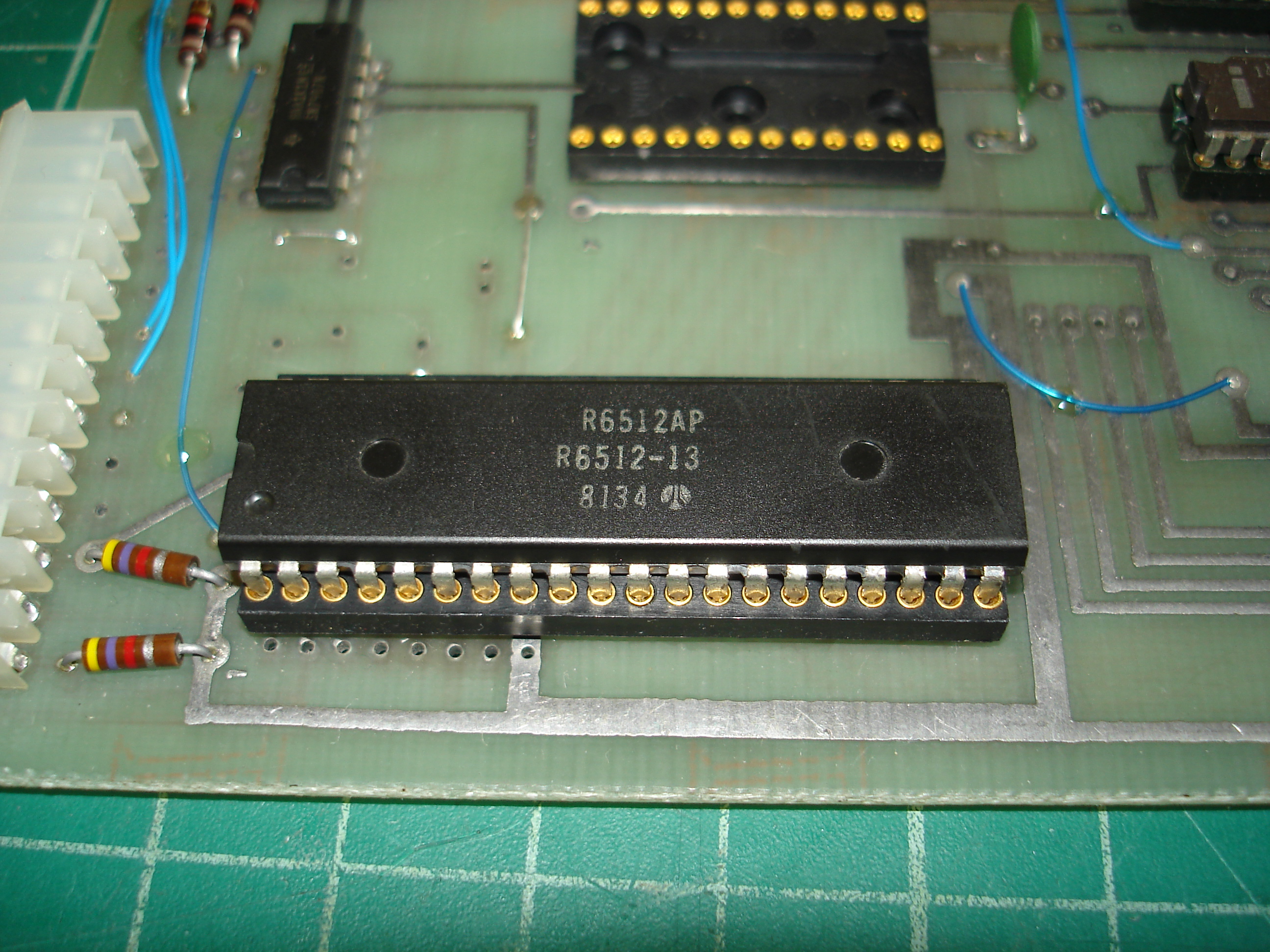
The R6512 does indeed work in this configuration! Pin 39, PHI2 OUT, is tied to ground when configuring the OSI 400 for Motorola 6800 or MOS 6501 operation, which is probably not great. I plan on replacing this hardwired jumper with a pair of machine pin sockets to allow the insertion/removal of a 24 AWG jumper.
With the R6512, the OSI 400 board can be built up to operate with Motorola 6800 compatibility, but can be switched over to a processor that supports 6502 compatibility and isn’t as rare or expensive as an actual MOS 6501. The R6512 also has a properly functioning ROR instruction! This is, in my opinion, the best of both worlds. While we do have reproduction OSI 400 circuit boards available, the 400 board is still not a trivial board to assemble, so being able to have just one configuration with no major changes is a definite bonus!
MOS 6501 CPUs tested