Topic: 64K RAM for the OSI Bus
Date: 2016 MAY 17
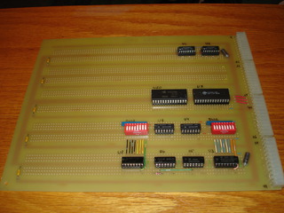
With the 32K OSI RAM board working, I decided to expand it to a full 64K using the expandable features I’d planned into the original 32K board. Built on the same OSI 495 prototype board as the original, this 64K expansion requires minimal modification to the 32K board, and the addition of three additional ICs, including the 32K x 8 static RAM.
We’ll only look at the additions to the 32K RAM board, so if you haven’t read that writeup, either head there now or look over the full schematic first. Clicking any schematic image below will take you to the full PDF, or you can download it here.
Segment Selection
Segment selection for the upper 32K is very similar to the lower 32K, with one exception: A15 is inverted, such that the 32K SRAM occupies the top half of the 64K address space. This lets us enable the upper 32K in 4K increments, just as with the lower 32K. In addition to mapping around ROM and I/O devices, this allows the board to occupy 0xD000 - 0xEFFF, which is required for OSI CP/M with the 510 CPU board.
The /MM line is again left for possible memory management expansion. If you’re not using memory management (most OSI systems aren’t), just tie it to ground for now.
Data Direction Generator
The Data Direction generator from the 32K board is modified for 64K by removing the connection to pin 1 of U6 and instead using the NOR of /CE1 and /CE2. This NORed value can be generated using another element of the 74LS00 at U6, as shown:
This will cause DD to pull low for any reads in any of the enabled 4K segments, regardless of whether they’re in the lower or upper 32K of the board’s capacity.
The Static RAM
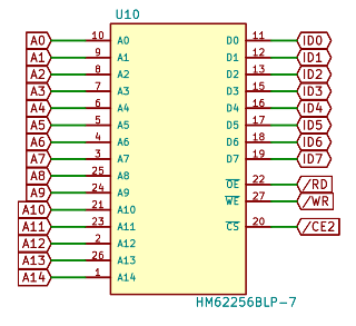
This board adds another 62256 JEDEC-compatible static RAM. It’s a 32K x 8 part that’s common, widely available, cheap, and easy to work with. It’s available in fast enough speeds that no wait states are required for any of the three processors available on my 510 CPU board. Wiring is straightforward:
All connections to the upper 32K are bussed to the lower 32K except for /CS, which is fed from the segment selector for the upper 32K.
Building the Circuit
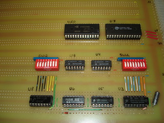
If you’re building this circuit on an OSI 495 prototype board, you can follow my layout for IC locations. The locations are labeled corresponding to the provided schematic, and pin designations should match, too.
Expansion started with the addition of three sockets: a 28-pin socket for the SRAM, a 16-pin socket for U8, and a 14-pin socket for U9. Be sure to connect the Vcc and GND pins to +5 and GND, respectively, on the prototype board. I typically use a cut off component lead soldered to the pad and trace, and clipped to length. If you bend the component lead into an “L” shape, you can hold the upper part of the “L” with pliers while soldering the lower part down. Clip off excess lead length with close diagonal cutters.
Since the new SRAM at U10 was mostly bussed directly to the existing SRAM at U7, I went ahead and connected it up first. Make sure to skip pin 20 on the new SRAM – this will be fed from the segment select circuit for the upper half of memory. The segment select circuit is almost identical to the circuit used in the 32K RAM board, except that pin 4 of the 74LS138 is fed with the inverted /A15. As you can see from the pictures, my layout of SW2, U8, and U9 mirrors that of the 32K layout. Don’t forget to connect U8 pin 5 to ground if you’re not using memory management!
With the new chips laid down, it’s time to modify the old Data Direction generation circuit. Remove the wire from U4 pin 8 to U6 pin 1, then wire in the new circuit that combines /CE1 and /CE2.
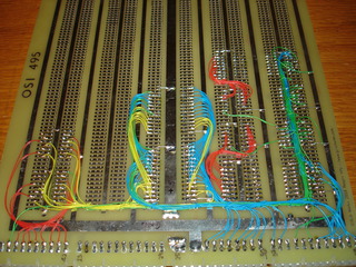
Here’s a full view of the back of the finished prototype:
Colors are the same as used with the 32K build:
- Blue is address, unbuffered directly from the OSI bus
- Yellow is internal data bus
- Green is control signalling
- Red was used for both the OSI data bus and between SW1 -> U4, SW2 -> U9
Check everything over with a multimeter or continuity tester, install all ICs, enable the 4K segments you want to use (SW2 on == segment enabled), and install the board in your Ohio Scientific. Power on and find out if you’ve got any wiring errors! Please let me know if you build one of these boards, if you have problems, or if you’d like to buy a 495 board for it.
memory errors avoided


