Topic: 32K RAM for the OSI Bus
Date: 2016 APR 23
Now that I have a few OSI 495 prototype boards on-hand, I could finally build a combined static RAM board for the Challenger III using modern static RAM devices. Finally, no more reseating a ton of SEMI4200s every time the Challenger was moved onto or off of the workbench! I decided to start with a 32K design, but design in such a way that it could be expanded to 64K and beyond without too much trouble.
This 32K RAM board design is suitable for anyone who needs to add to the base memory on a smaller Ohio Scientific system. It has been designed such that the board resides from 0 - 32K in address space (0x0000 to 0x7FFF). Each 4K segment in that range can be independently enabled or disabled – this allows one to retain small chunks of original system memory without having to disable it or alter the RAM board to prevent address conflicts. For exmaple, if you’re expanding a system based around the 500 CPU board, which has already been expanded to 4K RAM for BASIC, you can disable the bottom 4K on this design with a simple DIP switch setting.
On to the design! We’ll look at the five distinct blocks of the RAM board in detail and cover general construction techniques, assuming you’re also using a OSI 495 protoboard. Clicking any schematic image will take you to the full PDF, or you can download it here.
Segment Selection
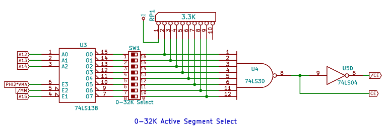
The segment select circuit does quite a bit of the work in generating the chip select signal for the static RAM and bus drivers. It’s based around a 74LS138 1-of-8 decoder IC, a very useful device with one active high and two active low enable inputs. This single device lets us break up the bottom half of address space into 4K segments, only generate a signal when A15 is low, and qualify the signal with Φ2•VMA.
We’ll start at the left and work our way right. Φ2•VMA (PHI2*VMA in the schematic) is the OSI bus line that signals that the address lines and bus direction lines are stable and a memory access can begin. It serves as the positive enable for the 74LS138. A15, the high address bit in a 64K system, is fed into one of the negative enable lines on the 74LS138 – this activates the IC only when A15 is low, indicating a memory request in the 0x0000 to 0x7FFF range.
The /MM line is left for possible memory management expansion. If you’re not using memory management (most OSI systems aren’t), just tie it to ground for now.
A12, A13, and A14 are fed into the 74LS138 as address inputs. The value on these three lines will determine which output of the decoder is active. Since the outputs are active low, all outputs will be high unless a segment is selected. The outputs go through an 8-position DIP switch to allow individually selecting whether a segment is enabled or disabled. From the DIP switch, the outputs go into the inputs of a 74LS30 8-input NAND gate. Pull-up resistors are required (some 1K - 10K value, I had 3.3K resistor packs on hand) so that the lines are pulled up if a switch is open.
The 74LS30 8-input NAND gate will output an active high Chip Enable signal – since it’s NAND, the output will be low only if no segment is active. When any segment becomes active, it will go high. This is inverted to give us /CE, an active low Chip Enable required by the static RAM.
/RD and /WR Generator
This one’s super simple – the R//W OSI bus line simply signals whether the memory access is going to be a read or write. It’s high for read, low for write. Our static RAM requires separate active low signals, and we make use of them elsewhere in the decode circuitry. Two inverter elements of a 74LS04 are used for this.
Data Direction Generator
The OSI bus is kind of confusing in that the peripheral boards are responsible for controlling the CPU board’s data bus buffers’ direction. This is referred to as DD on the bus, and is an open collector line. On most OSI boards, it’s driven from a regular totem pole TTL output through a diode, which effectively make it open collector.
DD is high for a write, and low for a read. It should only be generated when the board is active. We can combine /WR and CE from the above circuits into DD with a two-input NAND gate from a 74LS00. We’ll invert it through another section of a 74LS04 inverter for use in controlling the data bus buffers.
Data Bus Buffers
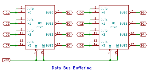
Ohio Scientific systems have two options for the data bus: active high or active low. Generally, a backplane system can use either, while some of the smaller Challenger machines require choices based on what the CPU board uses. For vintage boards, the usual choice is a pair of 8T26 inverting buffers for active low, or 8T28 non-inverting buffers for active high. My Challenger III uses an active low data bus, so I designed for 8T26 inverting buffers. They can be swapped directly for 8T28s, though with RAM data polarity doesn’t matter as long as it’s the same going in as coming out.
The /RE and DE inputs (Receiver Enable and Driver Enable, respectively) are both tied to /DD. This means that the buffers will be moving data from the system bus onto the internal data bus any time the board is not being read from, including when the board isn’t selected! This doesn’t matter as the static RAM won’t accept writes from the internal data bus unless /WE and /CS are both low.
The Static RAM
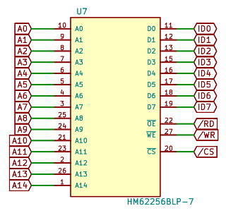
I chose to use a 62256 JEDEC-compatible static RAM for my board. It’s a 32K x 8 part that’s common, widely available, cheap, and easy to work with. It’s available in fast enough speeds that no wait states are required for any of the three processors available on my 510 CPU board. Wiring is straightforward:
The static RAM’s address lines go directly to the OSI bus. There’s no buffering as the buffer would present just as much of a load (possibly more) as the SRAM. /CE is accidentally labeled as /CS in the above figure. /RD and /WR come directly from the read and write generator above. Being as the 62256 is JEDEC pinout, it’s possible to plug in a 27256 EPROM instead of a SRAM. Since individual 4K segments can be enabled or disabled, this can be a quick way to put 4K ROM BASIC into an OSI system that lacks sufficient ROM sockets on the CPU board – a 400 board, for instance.
Building the Circuit
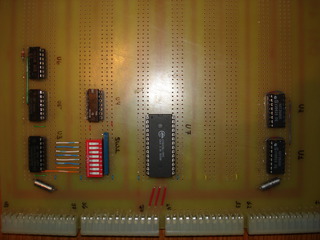
If you’re building this circuit on an OSI 495 prototype board, you can follow my layout for IC locations. The locations are labeled corresponding to the provided schematic, and pin designations should match, too.
I started with the +5 bridge near the edge connector – it’s a single-sided board, so the only way to cross the ground trace is with a jumper. I found it helpful to label the +5 and GND rails on the copper side of the board. Be sure to add small bypass capacitors at the top of the board and one or two larger electrolytic or tantalum capacitors near the bus connector – I used 0.1 uF ceramic capacitors at the top and 22 uF @ 10 V axial tantalums near the bus connector.
As you install each socket, be sure to connect the Vcc and GND pins to +5 and GND, respectively, on the prototype board. I typically use a cut off component lead soldered to the pad and trace, and clipped to length. If you bend the component lead into an “L” shape, you can hold the upper part of the “L” with pliers while soldering the lower part down. Clip off excess lead length with close diagonal cutters.
Next, I installed the sockets for the bus buffers, U1 and U2, and wired them to the bus. All of the underside wiring was done with 30 gauge Kynar wire wrapping wire. After the bus drivers were wired to the OSI bus, I added sockets for U3, U4, U5 and U6, as well as the DIP switch and resistor pack. U3 was placed so that most of the lines were a straight across connection to SW1. To keep the back of the board open for bus wiring, I made the connections from U3 to SW1 on the top, using 24 gauge wire from 25-pair telecom cable (solid conductor Ethernet cable works well, too). The resistor pack above SW1 can be mounted directly above SW1, since the 495 board uses triple hole pads. SW1 was then connected to U4 with more Kynar wire.
From here, I laid down all of the control signal wiring. This started with four address lines from the OSI bus to U3, along with Φ2•VMA. Don’t forget to tie /MM to ground if you’re not going to build memory management circuitry! Connect up R//W to U5, and jumper U5 pin 2 to U5 pin 3 to form the /RD and /WR generator. Make the connection from U4’s output to U5 as well, and the Data Direction generator can be built. I added the 1N4148 diode horizontally from U6 pin 3 to the free pad to the left of U6 pin 1, and ran a long wire to DD on the OSI bus.
Now comes the long, tedious bit of wiring. Solder down the socket for U7, the static RAM. I brought the /DD control line from the Data Direction generator to the bus buffers, then the control lines to the static RAM, then the internal data bus from the drivers to the static RAM. Address lines to the static RAM got laid in last – since there’s 14 of them, they take up more space and would probably have been harder to work around.
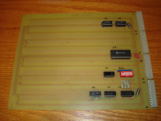
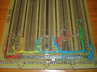
Here’s a full view of the back of the finished prototype:
Colors are as follows:
- Blue is address, unbuffered directly from the OSI bus
- Yellow is internal data bus
- Green is control signalling
- Red was used for both the OSI data bus and between SW1 and U4
Check everything over with a multimeter or continuity tester, install all ICs, enable the 4K segments you want to use (SW1 on == segment enabled), and install the board in your Ohio Scientific. Power on and find out if you’ve got any wiring errors! Please let me know if you build one of these boards, if you have problems, or if you’d like to buy a 495 board for it. Next, we’ll expand the board to 64K and discuss memory management! For now, enjoy 32K of problem-free static RAM for your Ohio Scientific!
memory errors avoided
