Topic: Preparing to expand the OMS-02 6507 SBC
Date: 2026 AUG 16
After cleaning up the OMS-02 6507 SBC, I wanted to start work on modifications for future expansion. Mostly I was interested in adding parallel I/O, but I also wanted to change the memory map a bit, to make the ROM fully accessible through paging, and gain more RAM at the same time. I started off with a simple change: the power inlet connector was changed from a Molex KK-100 series connector, to a right-angle Phoenix Contact connector:
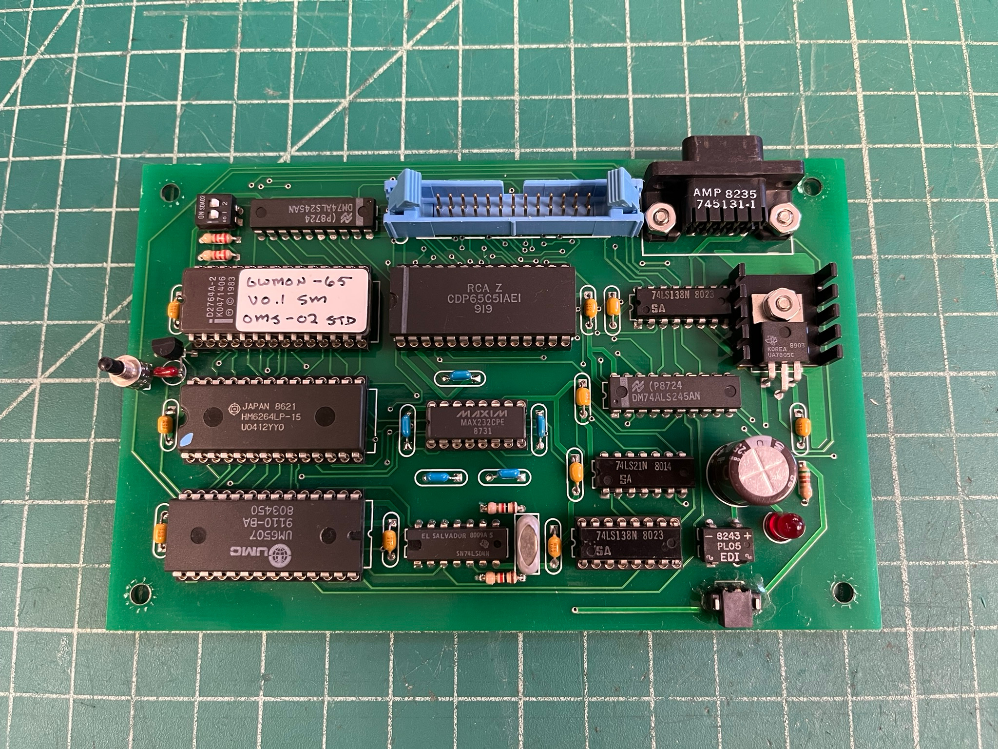
I chose a connector that was different enough that I wasn’t likely to mix up regulated and unregulated power, since the add-on board would be getting regulated +5V DC instead of using local regulation, as the OMS-02 does.
Memory Remap
The bulk of the modifications requiring rework are for the memory remap work. I didn’t want to just cut and jump, permanently altering the OMS-02’s memory map. There was also a constraint on the number of signals I could get off of the board: I was planning on pulling U3, a 74LS138, for the modifications, and I was planning on cutting some of the extra ground pins on the expansion header, but I was still limited to four or maybe five pins that could be freed up on the connector.
With those constraints, I settled on the following memory map changes:
- ROM available in 1K segments
- ROM switchout possible
- I/O to occupy a 1K segment
- RAM infill for the rest of memory space
The above will give me 6K of usable RAM with the ROM switched in, and an additional 1K segment with the ROM switched out.
Using U3’s footprint would give me the upper address lines, selects to RAM, ROM, and the I/O decoder (U4), and PHI2 from the 6507. RAM would need to have its A12 pin connected to processor A12 instead of SW2. ROM would need to have A10, A11, and A12 controlled by the expansion board. Three lines would need to go offboard for this – just the ROM’s upper address bits. I decided to make it reversible, and default to the original memory map, by using a 74LS157 2-to-1 multiplexer (excuse the scan quality, our scanner doesn’t like my engineering pad, apparently):

The SEL signal on pin 1 of the 74LS157 will determine whether we’re using the original memory map, or the modified one. It’s pulled up through a 2K2 resistor to +5V, so when nothing is connected to the expansion header, the system will operate with the original memory map. Pulling SEL low causes the board to use the new memory map. The modifications were fairly easy to implement with a 74LS157 in SOIC-16 package, epoxied to the bottom of the SBC:
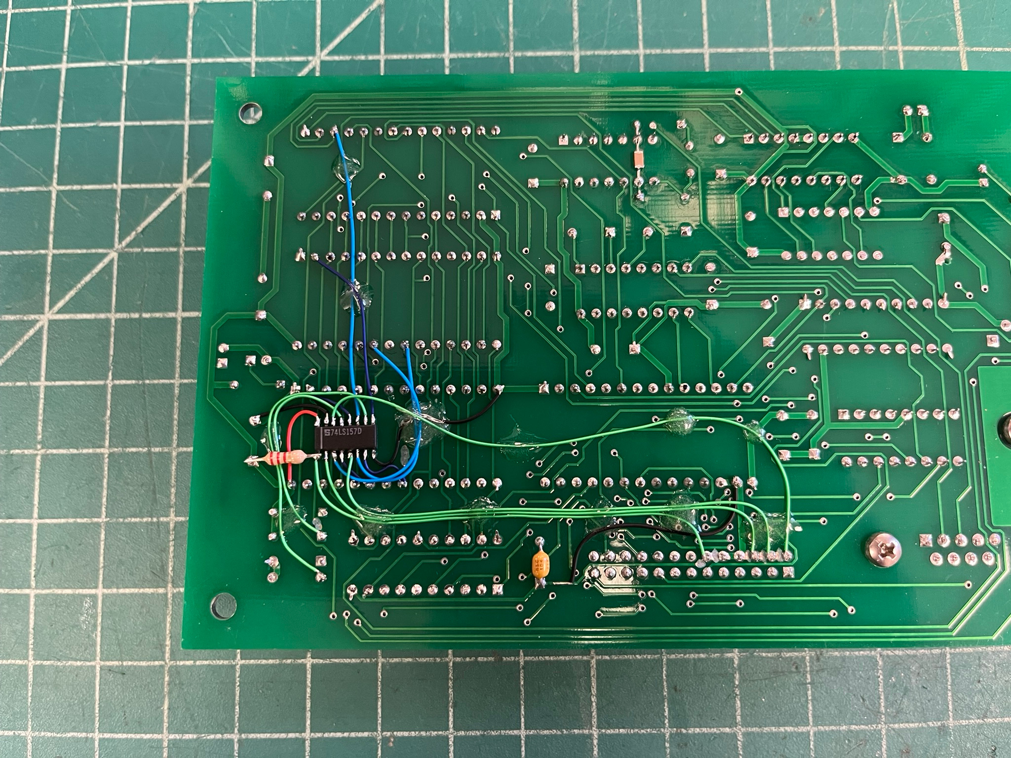
The following cuts were required for the ROM portion of the circuit:
- Cut
A12(pin 2) to DIP switch #1/2K2 resistor (bottom) - Cut
A11(pin 23) to processorA11(top, under socket) - Cut
A10(pin 21) to processorA10(bottom)
Only one cut was required for the RAM portion:
- Cut
A12(pin 2) to DIP switch #2/2K2 resistor (top, under socket)
With the cuts made, the flywires were run, as seen above. Red and black are +5V and GND, respectively. Light blue wires carry processor address lines. Purple wires are multiplexer outputs. Green wires are control. The 2K2 pull-up to SEL was made with a 1/4W axial resistor.
Expansion Board and Mounting Box
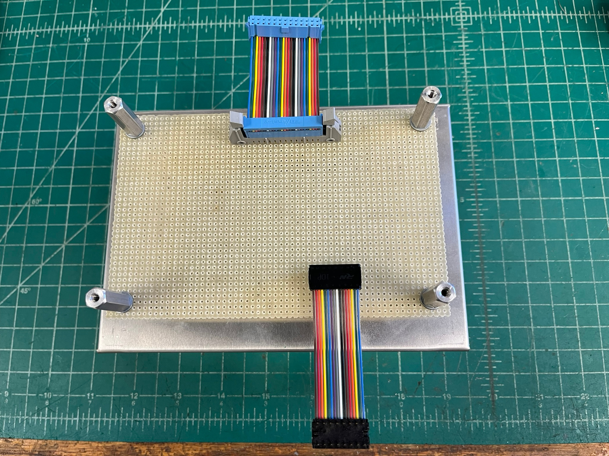
I set up a chunk of perfboard for the expansion board. I have a bunch of this vintage Vector perfboard, which has no copper on it at all. This is usually somewhat annoying to use, but with wire wrap, it’s not bad! I mounted a dual-row header and a 16-pin DIP socket with holes for mounting screws:
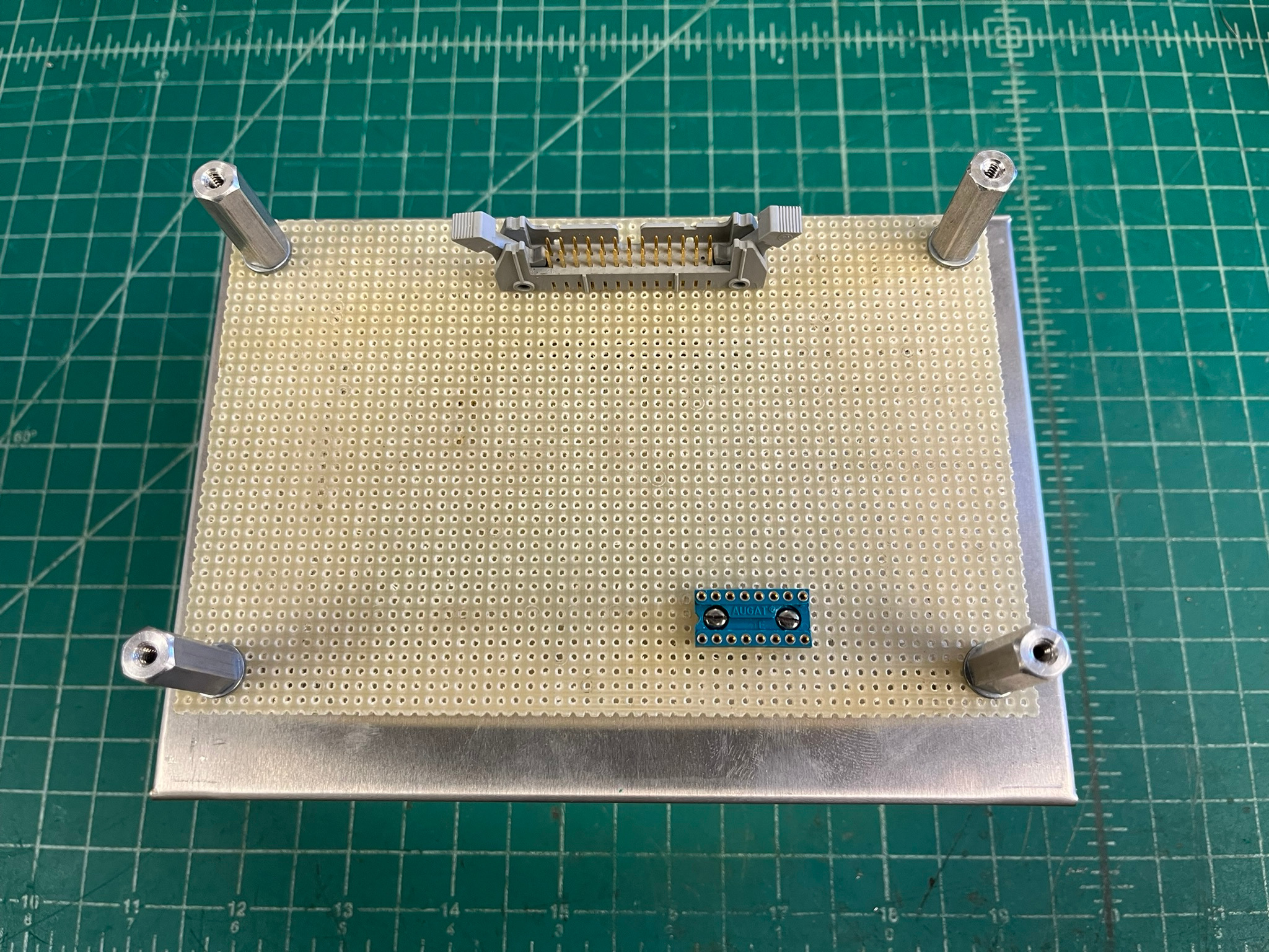
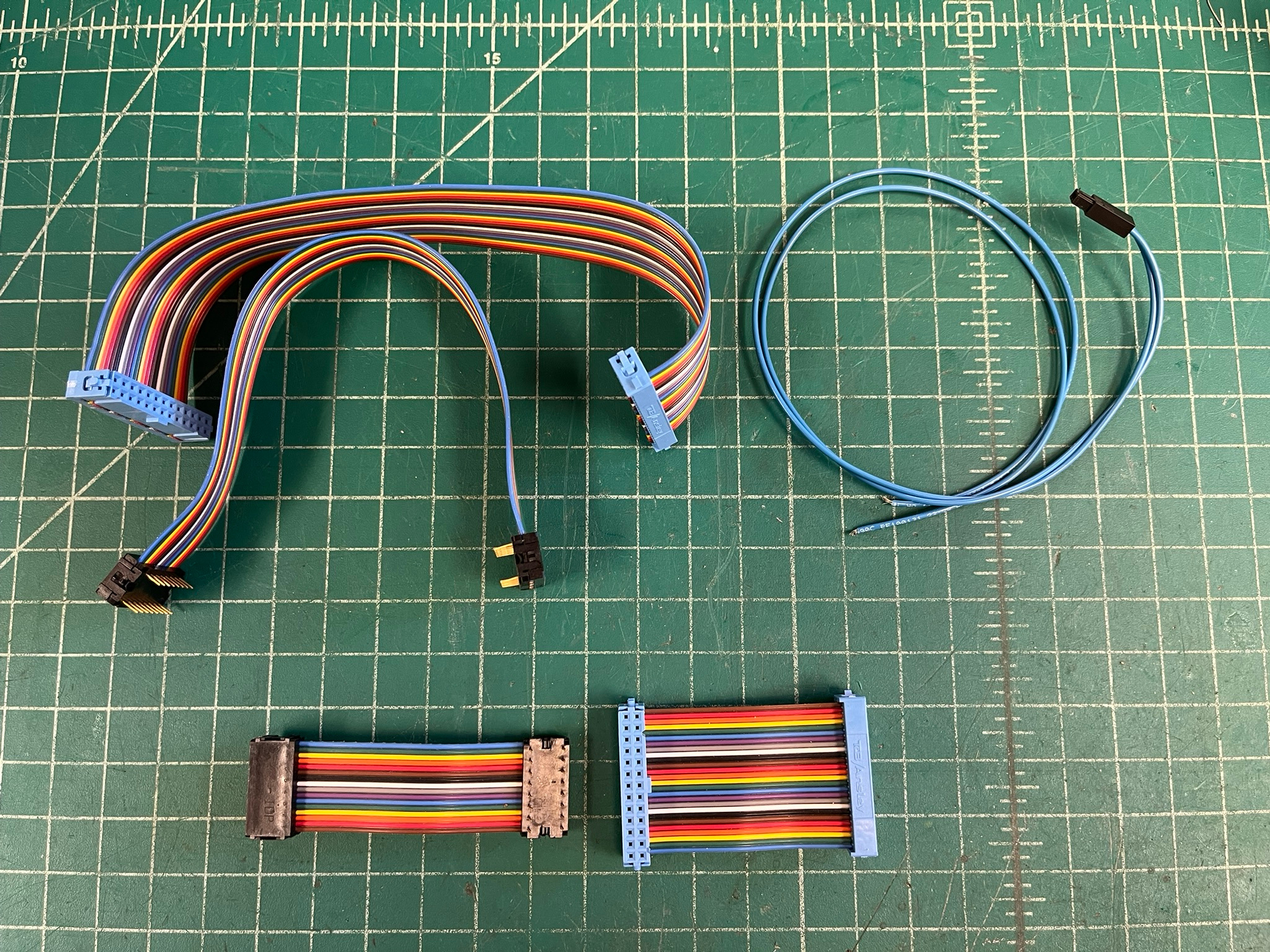
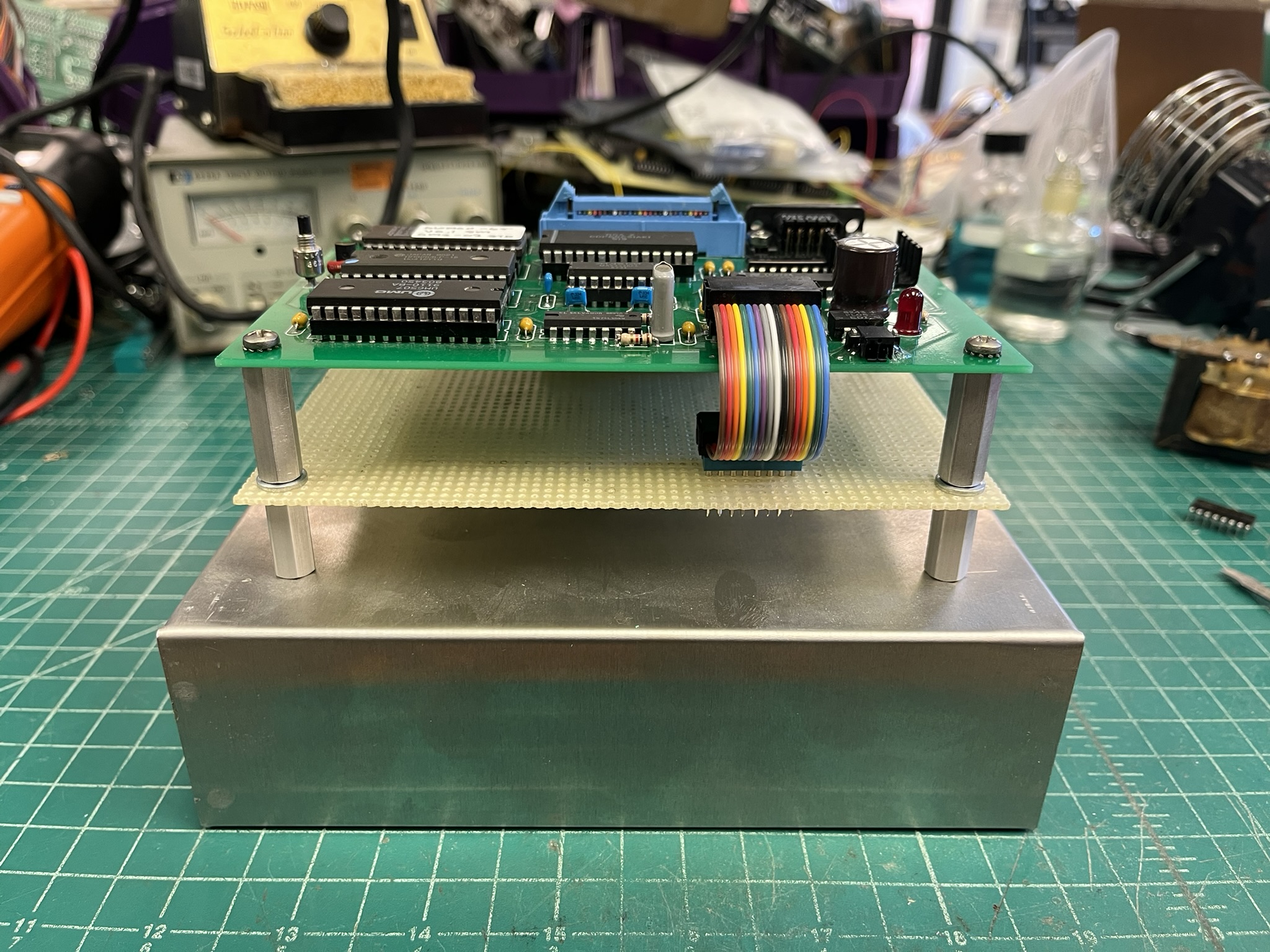
The whole thing mounts on a BUD chassis box, which will house the power supply and any I/O. The header at the top will connect to the expansion header on the OMS-02 SBC, and the DIP socket will connect via DIP plug to the socket for U3, the 74LS138 used for primary address decode. I made up two sets of ribbon jumpers: a long set for prototyping/development, and a short set for when the two boards are stacked up. Here they are, with the unregulated power inlet wire for the SBC:
The short jumpers will connect the two like this:
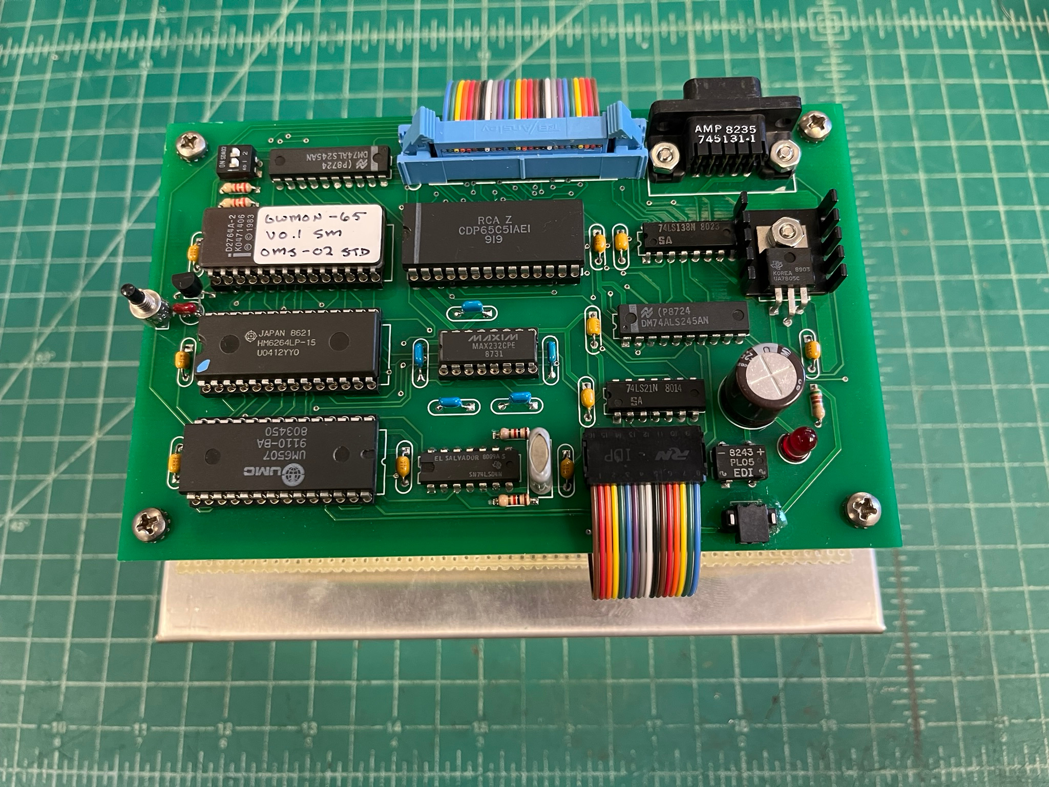
This makes for a reasonably compact package, while still letting me break the two boards apart on the bench for development work. The BUD chassis is tall enough to accommodate a transformer, capacitor, AC inlet connector, etc. Here’s a view of the full assembly, from the front:
I haven’t finished designing the circuitry for the expansion board yet. I will likely use a 6522 VIA, because what’s a 6502 core without a VIA, right?! I have several panel mount LED display holders that might work well in the base chassis, so those might get wired in too. Mostly, though, I wanted to add some parallel I/O for benchtop experiments.
SBCs expanded