Topic: REing the Identicon 8080 board
Date: 2026 AUG 10
Back in 2012, Sark and I had hacked on some Identicon 8080 CPU boards and gotten them running short test programs burned into 2708 EPROMs. The ultimate goal was to build an expanded system, using the CPU board as-is, and do something useful with it. That would require more reverse engineering!
In 2018, I’d gotten an Intel MCS-80 System Design Kit and noticed the similarities with the Identicon 8080 CPU board, which prompted me to revisit it and clean it up for demonstration at VCF Midwest 2019. I took care of some little things that weren’t quite right with my 8080 board:
- Straightening the bend the board had from being in a scrap lot
- Replacing lower quality sockets with machine pin
- Fully socketing the 2111A SRAMs and testing them in another card
- Replacing some broken or missing ceramic capacitors
- General cleanup of the ceramic ICs on the board
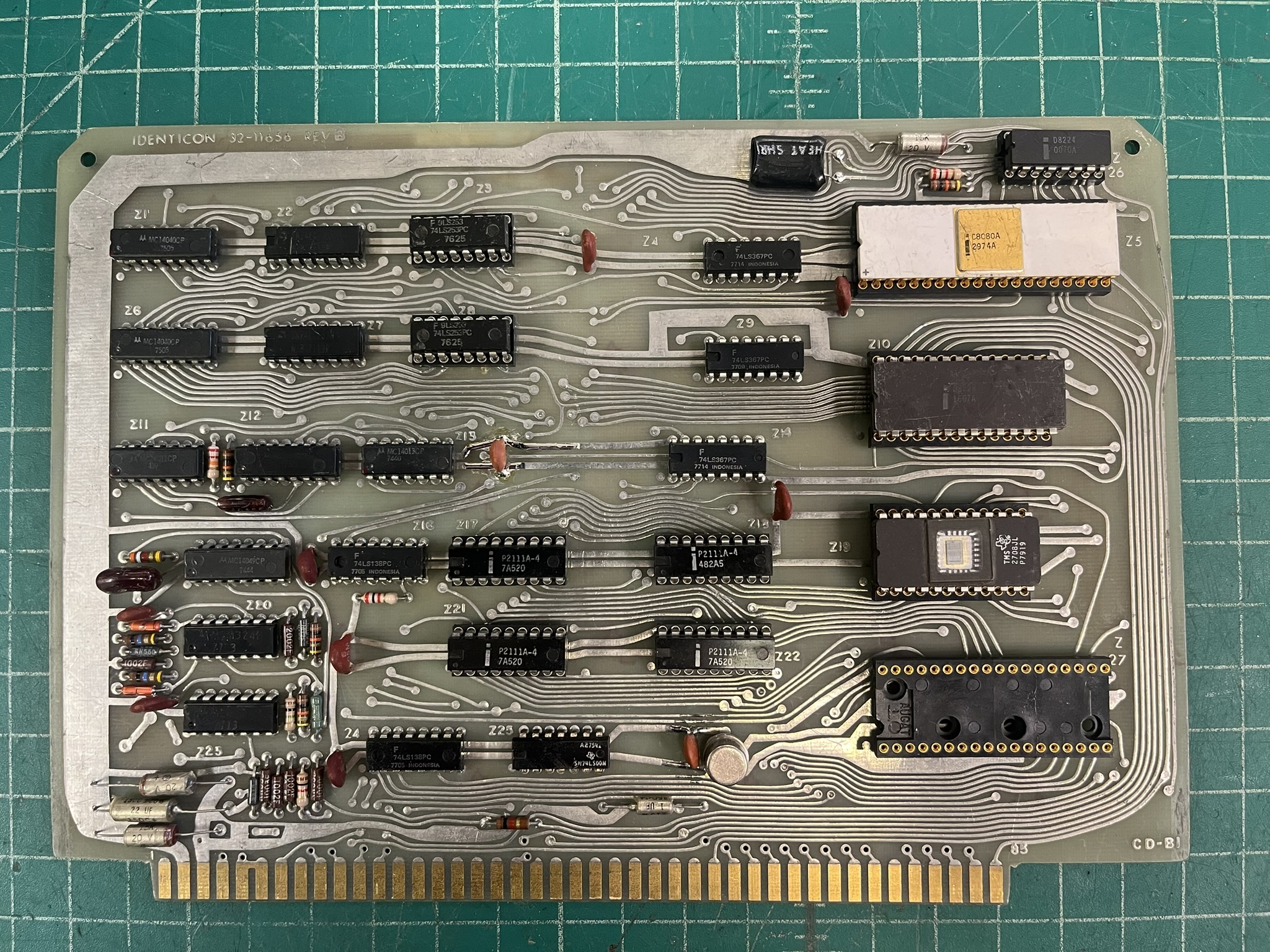
This is the board as it exists today:
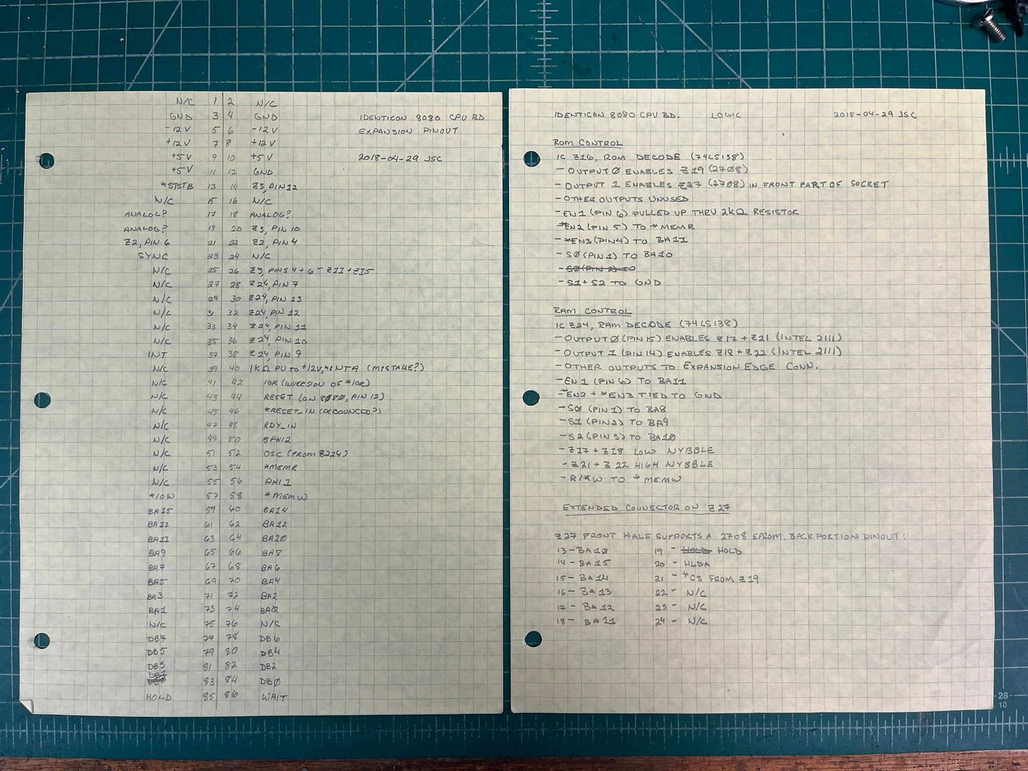
After the cleanup process, I spent a few evenings reverse engineering the board. I typically do so with the Simpson 260 multimeter and a pad of paper. The results look like this:
So, let’s go over what I figured out!
Edge Connector Pinout
I’ve traced all of the edge connector pins, these are their functions, as best as I’ve worked out:
  Identicon 32-11656 REV B 8080 CPU Board Expansion Connector Pinout
  ==================================================================

  Pin 1 is on the left end of the edge connector, on the component side,
  with the board held so the connector is down. Pin 2 is the left end on the
  solder side.

          SIGNAL   #     #   SIGNAL
      ---------------------------------
             N/C   1 o o 2   N/C
             GND   3 o o 4   GND
            -12V   5 o o 6   -12V
            +12V   7 o o 8   +12V
             +5V   9 o o 10  +5V
             +5V  11 o o 12  GND
          *STSTB  13 o o 14  Z3, PIN 12
             N/C  15 o o 16  N/C
         ANALOG?  17 o o 18  ANALOG?
         ANALOG?  19 o o 20  Z3, PIN 10
       Z2, PIN 6  21 o o 22  Z2, PIN 4
            SYNC  23 o o 24  N/C
             N/C  25 o o 26  Z3, PINS 4+6 -- Z11 + Z15
             N/C  27 o o 28  Z24, PIN 7
             N/C  29 o o 30  Z24, PIN 13
             N/C  31 o o 32  Z24, PIN 12
             N/C  33 o o 34  Z24, PIN 11
             N/C  35 o o 36  Z24, PIN 10
             INT  37 o o 38  Z24, PIN 9
             N/C  39 o o 40  *INTA, 1K pull-up to +12V
             N/C  41 o o 42  IOR (INVERSION OF *IOR)
             N/C  43 o o 44  RESET (ON 8080, PIN 12)
             N/C  45 o o 46  *RESET_IN (DEBOUNCED?)
             N/C  47 o o 48  RDY_IN
             N/C  49 o o 50  BPHI2
             N/C  51 o o 52  OSC (FROM 8224)
             N/C  53 o o 54  *MEMR
             N/C  55 o o 56  PHI1
            *IOW  57 o o 58  *MEMW
            BA15  59 o o 60  BA14
            BA13  61 o o 62  BA12
            BA11  63 o o 64  BA10
             BA9  65 o o 66  BA8
             BA7  67 o o 68  BA6
             BA5  69 o o 70  BA4
             BA3  71 o o 72  BA2
             BA1  73 o o 74  BA0
             N/C  75 o o 76  N/C
             DB7  77 o o 78  DB6
             DB5  79 o o 80  DB4
             DB3  81 o o 82  DB2
             DB1  83 o o 84  DB0
            HOLD  85 o o 86  WAIT

  N/C means "No Connection"
  Signals with * in front are active-low.
  Signals with a B in front (or after the splat) are buffered
The bus structure is fairly sane. the Z numbers refer to IC designations on the board. I have not yet drawn up a schematic for it.
Note that the 1K pull-up to +12V on *INTA puts the system in simple interrupt mode.
Z27 Extended Connector
IC socket Z27 is a bit odd, it is 36-pin, but it holds a 2708 EPROM justified toward the pin 1 end. Here’s its pinout:
  Identicon 32-11656 REV B 8080 CPU Board Socket Z27 Pinout
  =========================================================
                          _____   _____
                         |     \_/     |
                   BA7  -|  1       36 |-  +5V
                   BA6  -|  2       35 |-  BA8
                   BA5  -|  3  Z27  34 |-  BA9
                   BA4  -|  4       33 |-  -5V
                   BA3  -|  5       32 |-  *CS
                   BA2  -|  6       31 |-  +12V
                   BA1  -|  7       30 |-  GND
                   BA0  -|  8       29 |-  DB7
                   DB0  -|  9       28 |-  DB6
                   DB1  -| 10       27 |-  DB5
                   DB2  -| 11       26 |-  DB4
                   GND  -| 12       25 |-  DB3
                  BA10  -| 13       24 |-  N/C
                  BA15  -| 14       23 |-  N/C
                  BA14  -| 15       22 |-  N/C
                  BA13  -| 16       21 |-  *CS from Z19
                  BA12  -| 17       20 |-  HLDA
                  BA11  -| 18       19 |-  HOLD
                         |_____________|

  N/C means "No Connection"
  Signals with * in front are active-low.
  Signals with a B in front (or after the splat) are buffered
Pretty interesting! Since all of the address bits are accounted for, and there’s HOLD and HLDA, I suspect this was a development/debug connector, which allowed accessing system memory from another system. The N/C pins could be used for something like *IOR and *IOW to make a flywire-less I/O device for testing.
ROM Control
IC Z16, a 74LS138, handles ROM decoding:
- Output 0 enabled Z19 (2708, socket below 8228)
- Output 1 enables a 2708 justified toward the pin 1 end of Z27
- All other outputs are unused
EN1(pin 6) pulled up through a 2K resistor*EN2(pin 5) to*MEMR*EN3(pin 4) toBA11S0(pin 1) toBA10S1(pin 2) andS2(pin 3) toGND
This gives us four usable decode pins for 1K devices. Only two are used, for the ROMs typically installed in Z19 and Z27. The others are not brought down to the edge connector.
RAM Control
IC Z24, a 74LS138, handles RAM decoding:
- Output 0 (pin 15) enables Z17 + Z21 (Intel 2111A)
- Output 1 (pin 14) enables Z18 + Z22 (Intel 2111A)
- Other outputs are run to the edge connector (see above)
EN1(pin 6) toBA11*EN2(pin 5) +*EN3(pin 4) toGNDS0(pin 1) toBA8S1(pin 2) toBA9S2(pin 3) toBA10
The above means that Z17 and Z18 are the low nybble. Z21 and Z22 make up the high nybble – the Intel 2111A devices are 256 x 4 bit. The SRAMs’ R/*W line is connected to *MEMW.
The unused outputs from Z24 being brought to the edge connector suggest that there may have been systems that needed more RAM, which would’ve been present on a separate card. Neither Sark nor I have such a board, so it’s impossible to know for sure!
Final Thoughts
The Identicon 8080 CPU board’s bus pinout is fairly sane and should be easy to expand. I will probably add flywire modifications to allow finer grained control of onboard memory decoding, as the current circuitry is not fully decoding address space, which would make expansion more difficult, beyond the 2K of RAM decoded by IC Z24.
I still need to go through the I/O section of the board. The edge connector pins marked ANALOG? are likely part of the barcode wand interface, and may not be useful for other things. There’s still a handful of chips I haven’t made an attempt at reverse-engineering yet.
barcode readers reverse engineered