Topic: Maxing out RAM on the SDK-80
Date: 2019 APR 01
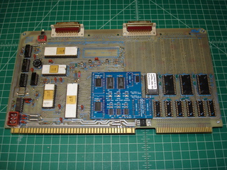
The Intel SDK-80 cleanup resulted in a functional SDK-80 board under both the MCS-80 ROM monitor and GWMON-80. The board was “maxed out” at 1K RAM in eight 2111/8111 type static RAMs. While 1K of RAM is sufficient for many small programs, it’s still not a lot of RAM. I wanted to add more memory to my SDK-80, but I wanted to do some experiments with the decode circuitry before committing it to the prototype area. I also thought that perhaps other hobbyists would like a RAM expansion board that required no permanent modification to the SDK80.
The original memory decode on the SDK-80 presents a challenge for any significant expansion. As designed, there are four unused chip select outputs from the 8205/3205 memory decoder, which will enable 256-byte pages, presumably for more 2111/8111 style SRAMs. That’s what the previous owner of my SDK-80 had done. Adding more RAM requires rework of the memory decode circuitry since ROM and RAM are not fully decoded: they repeat throughout memory. One solution is to pull the memory decode ICs and just drive their output lines with new decode circuitry. Another possible solution involves cutting some of the 8205/3205 enable lines and driving them with extra decode logic.
A third option, the one I chose to implement, is simply to design a board that plugs in and completely replaces the existing decode logic. This has the advantage of being fully reversible as long as the 8205/3205 decoders are socketed, which mine are. But, if we’re going through the trouble of designing a mezzanine module to replace decode, why not enhance it and provide more functionality on the module itself? I came up with the following design goals:
- Provide more specific RAM and ROM decode
- Allow ROM to be relocated from
0x0000to0xF000 - Allow ROM to be completely disabled
- Provide as much RAM as possible on the mezzanine itself
- Support Ferroelectric RAM (FeRAM)
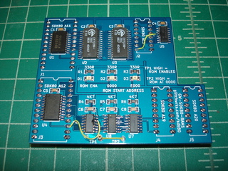
The first prototype of the module nearly succeeded in these goals, but due to a design error, ROM was relocatable but could not be disabled entirely. It also turned out to be easier to also replace the 8212 address bus buffers on the mezzanine:
The above image shows the first prototype, with some rework cut and jump fixes. The mezzanine replaces the following ICs:
- A11 and A12 (8212 address bus buffers)
- A13 8205/3205 ROM address decoder
- A18 8205/3205 RAM address decoder
- All 2111/8111 static RAMs
Replacement of the 8212 address bus buffers was accomplished with 74LS244 octal tristate buffers. These buffers are simply connected as 8-bit drivers, with the outputs always enabled. Using this approach made the board implementation simpler and kept the height down, since DIP packaged 8212s were not required to plug into the top of the mezzanine.
The mezzanine drives the chip selects for the onboard 2708 EPROMs using a 74LS138 1-of-8 decoder, just as in the original circuit. The big difference is the use of one of the 74LS138 enable inputs to make memory decoding more specific; that is, ROM does not repeat through memory space, it only occupies the 4K block to which it is assigned.
The signal for this enable is generated by a 74LS136, which is a quad Exclusive-OR (XOR) gate with open collector outputs. The outputs are all tied together and, with a pull-up resistor, form the active-low ROM ENA signal. On each XOR gate, one input goes to an address line, A12 through A15. The other inputs are tied together and pulled up with a resistor. The effect is to locate ROM at the standard address of 0x0000 when the signal at the pull-up resistor is high, and to relocate ROM to 0xF000 when the signal at the pull-up resistor is grounded.
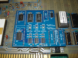
RAM is implemented using two 62256-type 32K x 8 static RAMs in SOIC packages. These are very common SRAMs; in fact, the two pictured were removed from the logic boards of dead IDE hard disks. RAM is enabled any time the EPROM decode circuit is inactive, resulting in 60K of RAM when the ROM is active, and a full 64K when the ROM is disabled. Since ROM disable did not work on this prototype, the board is limited to 60K of RAM. With ROM relocated to 0xF000, this is a very nice amount of RAM for running programs that would’ve been traditionally loaded via cassette or paper tape!
The bug in the design was an oversight in the ROM address decode: I’d attempted to run address line A12 into the 74LS138 ROM decoder directly, and used one of the XOR gate inputs as ROM disable. This caused a conflict between ROM and RAM in the first 32K of memory space. To overcome the problem, the A12 connection to the 74LS138 was cut and the input grounded (yellow wire in upper-right corner), The ROM ENA input to the 74LS136 was lifted and jumpered to A12 (yellow wire in bottom-left corner), and the two test points were tied together into a single point that locates ROM at 0x0000 when left disconnected, or 0xF000 when grounded. With the problems isolated, another prototype was run:
The second prototype works, and accomplishes all design goals, with no extra IC packages! Gates were economized by using a single gate to drive both ROM address LEDs (one sources current, the other sinks it) and using a 2N3904 transistor to drive the ROM ENA LED. Note that the SRAMs used on this build are much wider than the ones on the first prototype – they are also salvaged ICs, and the footprints laid out for this boar were intentionally designed to accommodate both regular 28-pin SOICs and the wider variety often found in mid-90s hardware.
The ROM remap and ROM disable inputs are intended to be driven by the 8255 PPI populated on the SDK-80. I haven’t implemented this permanently, a 40-pin DIP clip was used during testing to get the required signals. These signals are not strictly required: with TP1 and TP2 disconnected, ROM will be addressed at 0x0000 and enabled, and the rest of memory space will be RAM.
The second prototype still needs to be tested with FeRAM, the correct signal conditioning for *CS should be designed in already, but has not been verified. Once that is complete, GW-SDK80-RAM1 modules will be available for other hobbyists! With the GW-SDK80-RAM1 developed, additional expansion options for the SDK-80 can be developed…
SDK-80s expanded


