Topic: Checking out and fixing a MAI 8080 board
Date: 2026 AUG 03
Read down to the Initial Checkout section concerning a short on the -5V regulator before applying power to a MAI 8080A/9080A System Card – you can destroy part of your board if it has a short like mine did!
Bill Degnan had gotten out his MAI Jolt 6502 SBC at one of the workshops he hosted in the 2010s, and since then, I’ve had a saved search on a popular electronic auction site, waiting for a JOLT to show up. When I got a saved search alert in August 2025, and the image looked correct, I purchased it immediately. Imagine my surprise when I opened the package and saw this:
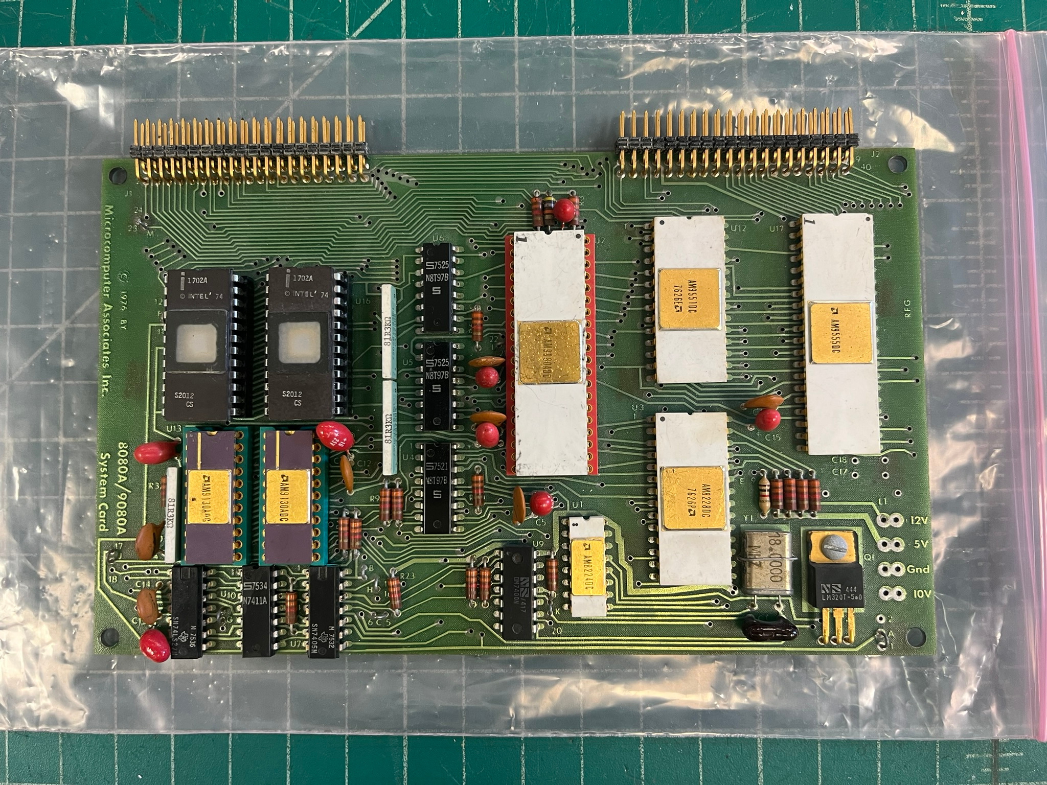
What had looked like a Super JOLT to me turned out to be something I’d never heard of, the 8080A/9080A System Card:
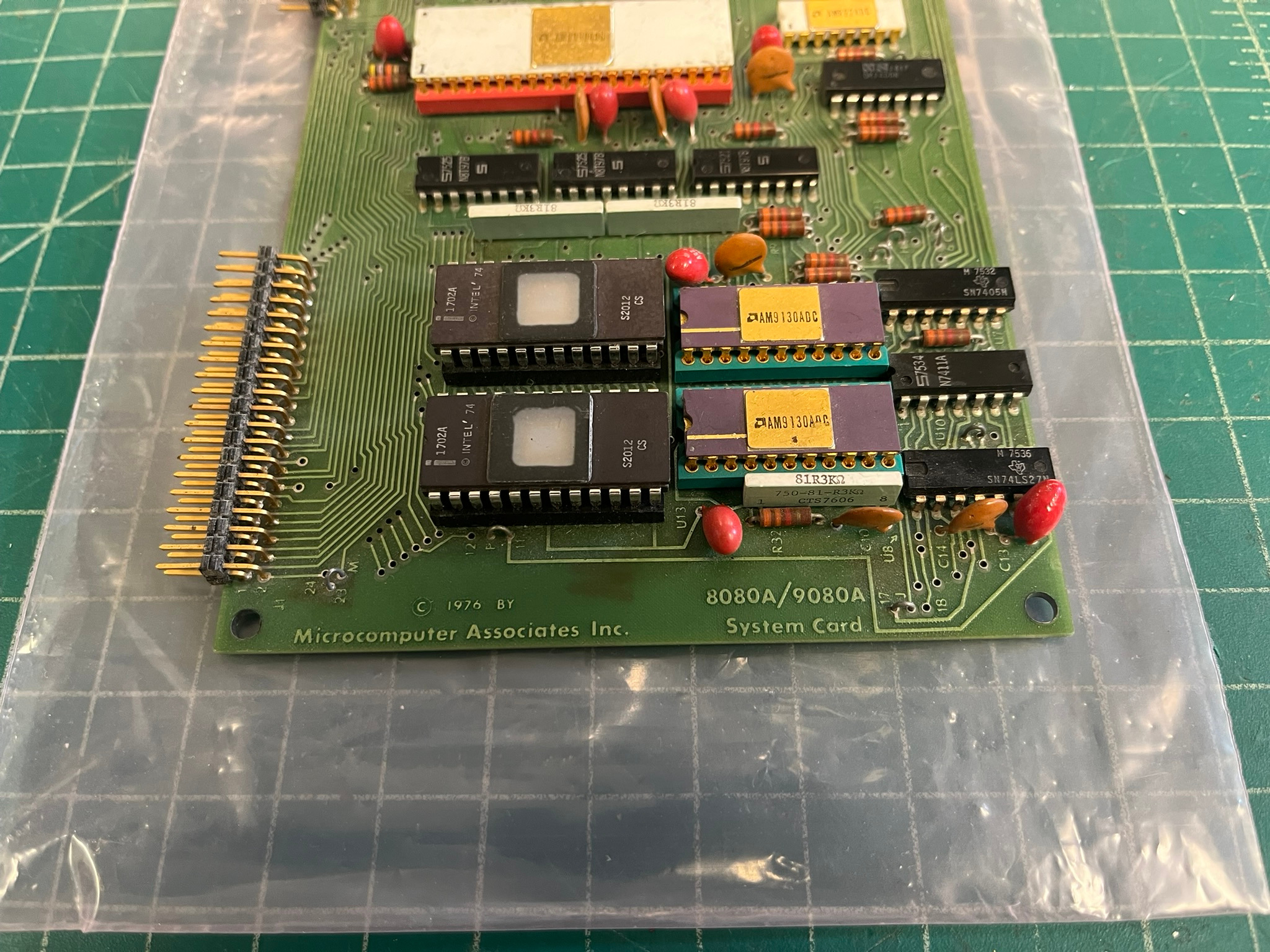
Interesting! Not what I expected, and I don’t know that I’d have paid what I paid for it if I’d realized that, but it was mine to hack on now, anyway! I also received an original paper copy of this MAI product catalog, which does show the 8080A/9080A System Card on PDF pages 12 and 13.
There is little information other than the above catalog pages and a note in the MAI newsletters concerning the 8080 SBC, and I haven’t seen any pictures of another one, other than those in the catalog and product announcements. It’s a fairly typical, compact, 8080 SBC with the following:
- 8080A at 2 MHz
- 8224 clock generator
- 8228 system controller
- 1K of static RAM
- 2K of UV EPROM or 4K of mask PROM
- 8251 USART
- 8255 PPI
Do note that the board I received came with Intel 1702A 256 x 8 UV EPROMs stuck in the sockets, but this is not a supported configuration on the 8080A System Card. I suspect the seller just stuck them in there to make the sale. I read them in the 1702/1702A programmer on the IMSAI 8080, and they were mostly blank, with a few flipped bits, probably from bit rot (they came with no labels). There was dust in the sockets under them:
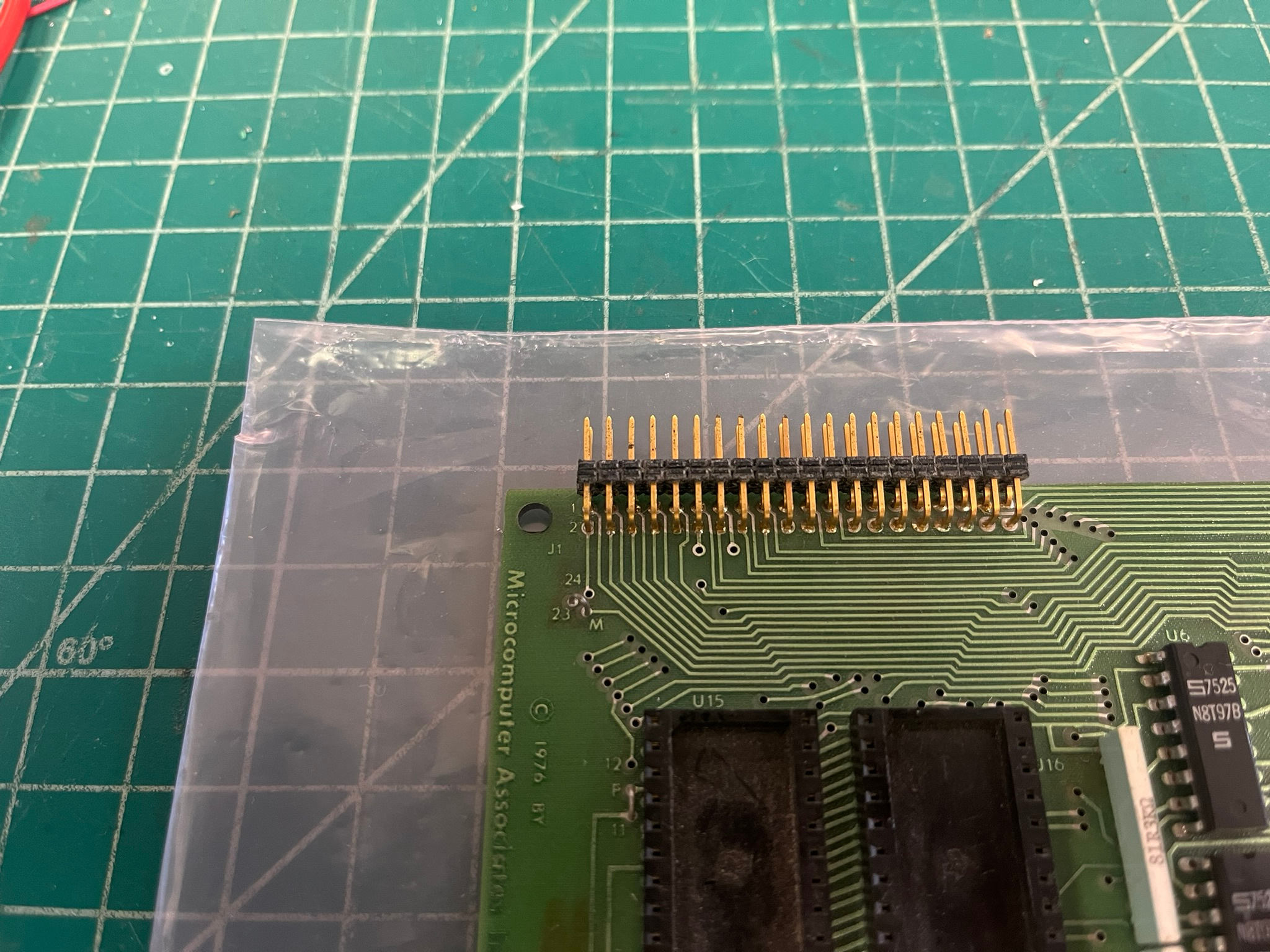
Since the SBC uses the MCS-80 family chipset, the system bus is quite sane, as compared to some of the “we don’t want to use the expensive MCS-80 chips” designs, which vary in how they transform the status output from the 8080 into bus signals. The system and application connectors are both 40 pin, and at least mimic the JOLT pinout, though I have not fully compared the two.
Here’s a look at the AMD second-sourced MCS-80 family chips:
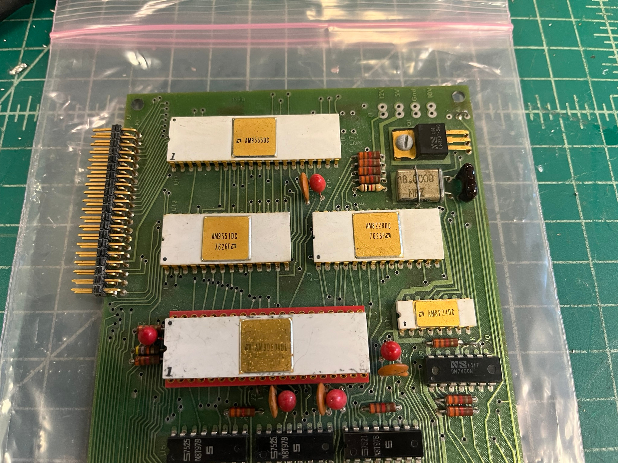
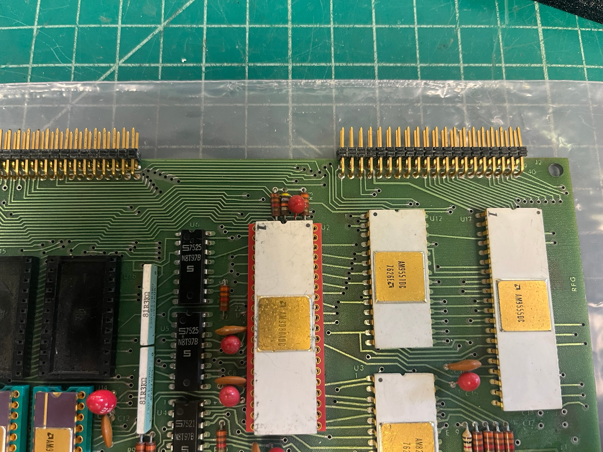
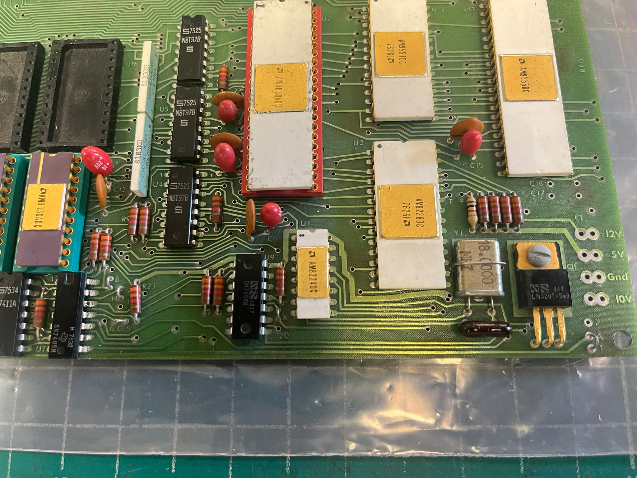
Soldering such expensive ICs was certainly a decision, but they do look nice! the PPI and USART both carry earlier AM95 prefix part numbers, though they are fully equivalent to the 82 prefix parts from Intel and other manufacturers. Here’s a closer look at the USART and system controller:
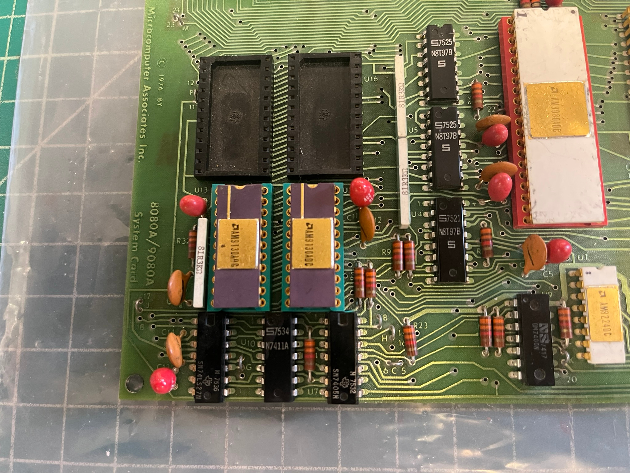
The 1K of onboard memory is provided by two AM9130 1K x 4 static RAM chips:
Now that we’ve had a look at the board in general, let’s see about getting it functional…
Initial Checkout
I spent a little time reverse-engineering the SBC with a Simpson 260 multimeter and pad of paper. My main objectives were to find out where ROM, RAM, and the USART live in address space. I traced out most of the decode circuit and found the following:
- ROM at
0x0000through0x0FFF - RAM at
0x1000through0x13FF - USART base address
0x00 - PPI base address
0x84
The above assumes jumpering for 2708 type 1K x 8 UV EPROMs – I haven’t fully documented the jumpers yet, but will post that information once I have.
I customized GWMON-80 for the 8080 System Card (the make target is mai) and burned it to a 2708 EPROM with the Data I/O 29B and UniPak 2B. Before applying power, I wanted to have a close look at the board to check for damage and shorts. I’m not sure if this board was ever powered up, as there was no evidence of solder on the power pads:
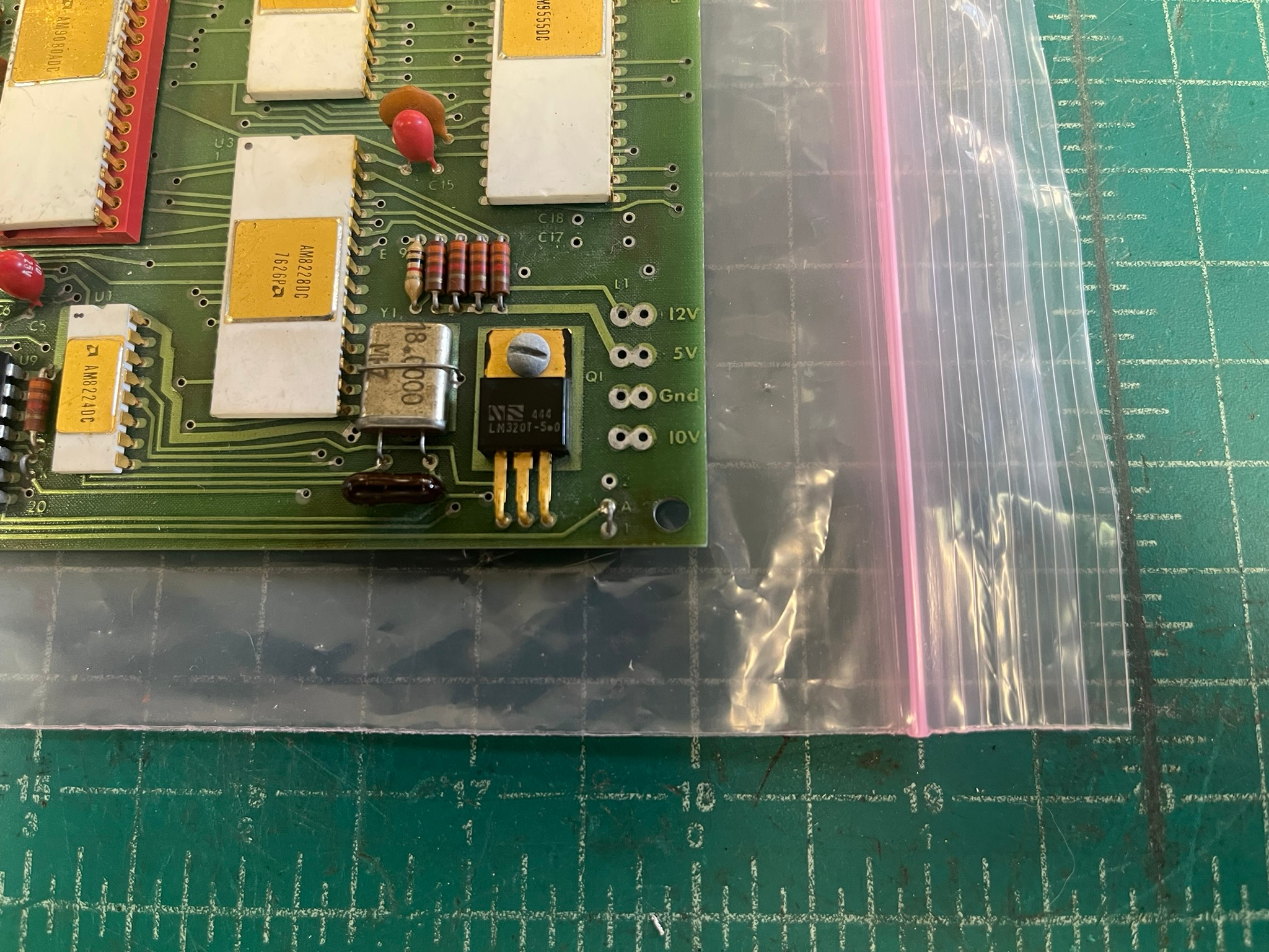
I pretty quickly found a major problem with the onboard -5V regulator: there’s a trace that runs far too close to the tab mounting hole, and looked like the spring washer was probably shorting the trace to the tab, which has unregulated -10V on it:
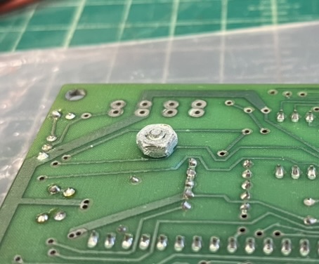
The Simpson 260 confirmed this was indeed a short. The trace it shorts to runs to the chip select line on the 8255 PPI. Powering it up like this would’ve been a disaster! I removed the screw from the -5V regulator, and found that there was still a short:
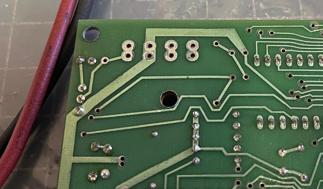
I’m not sure if this persistent short was caused by the spring washer smearing the trace and through-hole plating together, or if this is an etch defect as shipped from MAI. If it was an etch defect, there’s no way this board could have been tested at the factory or anywhere else. I’d originally planned on adding a nylon washer to the regulator tab screw, but due to the etch short, I tucked a mica insulator behind the regulator, and used a nylon #4-40 screw:
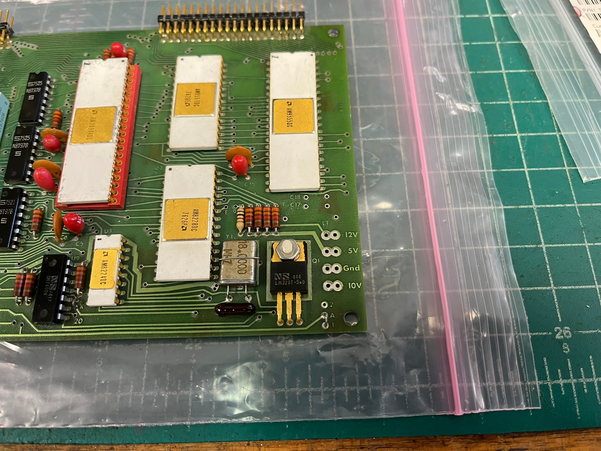
That cleared the short! I don’t know why the trace was run so close to the -5V regulator mounting hole in the first place, there’s plenty of room around it to have added a lot of clearance.
With the short resolved, the board was lashed up for testing:
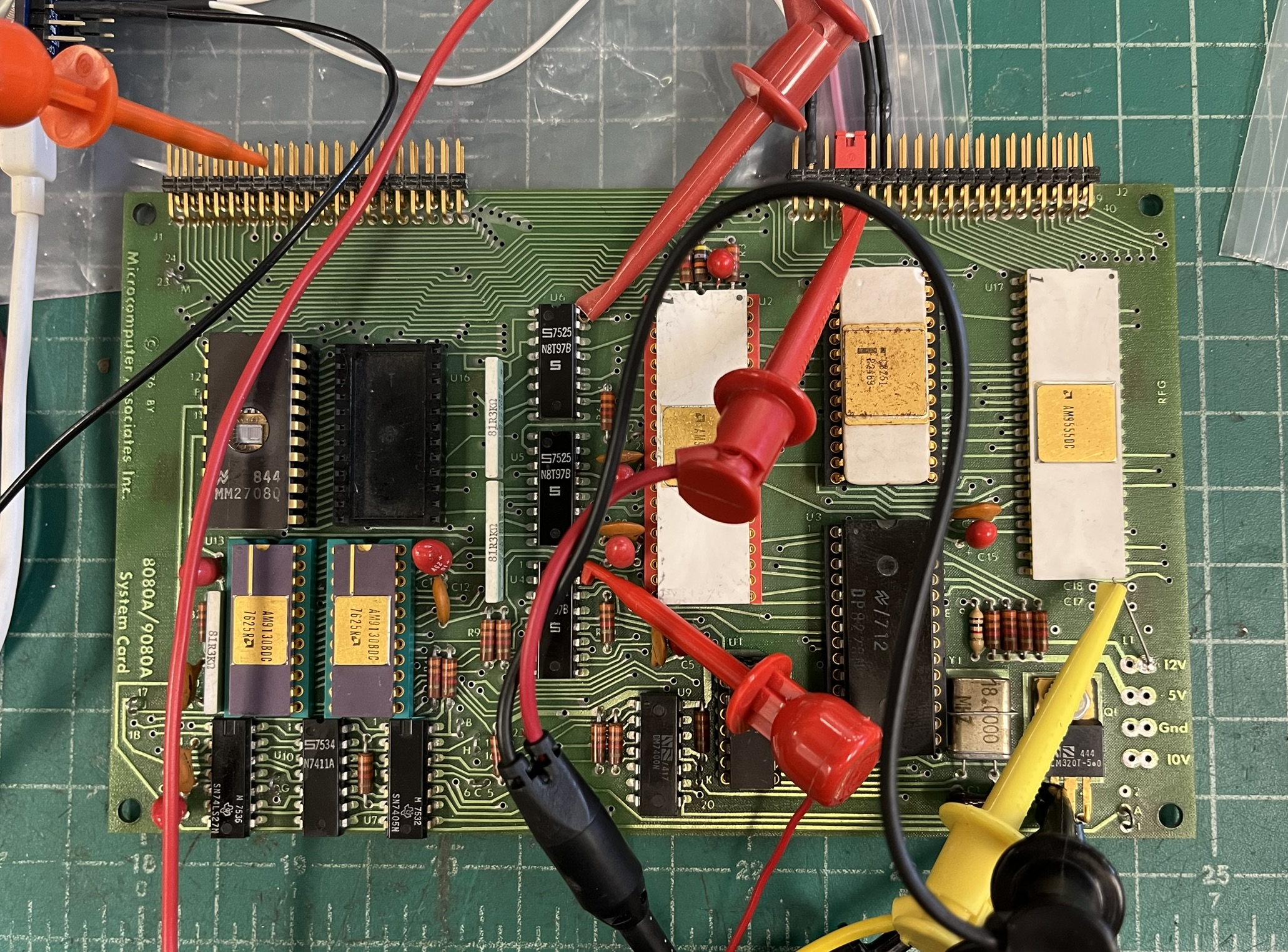
Power is injected at random points on the board, since no connector was soldered. I did have to add a snipped component lead to the 12V input, as there was nowhere convenient to grab on to. The application connector provides TTL serial (there’s no level shifting of any sort on the SBC), so it was connected to the previous version of an Adafruit CP2102N Friend USB to TTL serial converter. The CP2102N Friend had to be grounded to the power supply, as there’s no ground available on the application connector. Don’t forget to connect *CTS as the 8251 won’t talk without it!
There’s no bitrate clock on the SBC, and the 2 MHz system clock isn’t useful for that purpose, so it was provided by the Krohn-Hite 5920 Arbitrary Function Generator that lives on the workbench I was using:
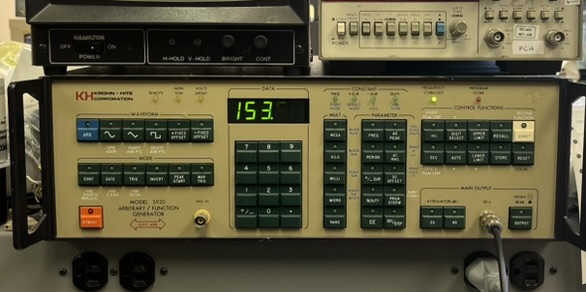
The generator is set to produce a 2.5V peak (remember: halve the amplitude if you’re not using a 50R termination!) square wave with fixed positive offset. Output frequency was set to 153.6 kHz, which gives 9600 bps with a divide-by-16 setting on the USART. The TX and RX clock pins were linked with a jumper shunt, since they’re next to each other on the application connector.
The GWMON-80 ROM was installed in socket U15, which is addressed from 0x0000 to 0x03FF, power was applied, the generator output was turned on, and…nothing!
Repairs
I hooked up the logic probe and started poking around the board. The processor had no address bus activity, and the reset line appeared to be stuck in reset. I found the reset pin on the system connector, and tried both grounding it and pulling it to 5V, but the reset remained stuck…guess it’s time to pull that soldered 8224 clock generator and replace with a socket!
I pulled out my testing Intel SDK-80, which also uses the MCS-80 family chipset, and stole its 8224 clock generator – it’s fully socketed, and tested, so it’d make a good source for known-good substitute parts. The SDK-80’s 8224 got me a system clock and reset signal, and now I had address bus activity, but the EPROM never selected. I traced the signal backwards through the logic, and found DBIN was never asserting. It wasn’t asserting on the 8228 system controller either, so that’d have to get desoldered, replaced with a socket, and borrow the one from the SDK-80…
Now I had a chip select activating to the EPROM, but still no serial activity. The USART was selecting, but didn’t seem to be getting initialized – the external TxREADY and TxEMPTY pins remained floating. Could the USART be dead, too? Desolder, replace with socket, steal from the SDK-80…yes, dead USART! Still no GWMON-80 output on the console…
This is a simple little board, so that pretty well left two likely culprits: a dead PPI messing up the data bus (it was at least not shorted, I could see data bus activity, and the USART was getting initialized), or bad AM9130 SRAMs. Since the SRAMs were already socketed, and we had some in the MISC STATIC RAM inventory, I swapped them. That was it! GWMON-80 signed on.
Testing with GWMON-80 confirmed my reverse engineered memory and I/O layouts, including that it is possible to have I/O conflicts, and that address line A15 isn’t considered in RAM/ROM decoding. I was unable to test the PPI though, it did not respond to reads or writes, and I couldn’t change the control register. I desoldered that too, installed a socket, and borrowed the 8255 from the SDK-80…and that fixed it. So, everything that touches the data bus, plus the 8224 clock generator, were all dead:
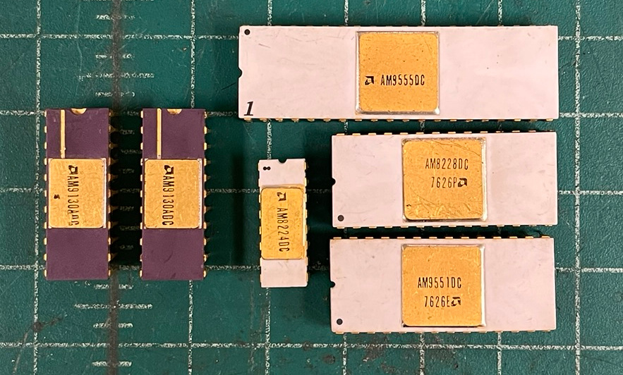
Well, that’s a bummer! I retested the MCS-80 family chips in the SDK-80, just in case, and they are all dead. Swapping the AM9130 ICs into the MAI SBC one at a time produced no GWMON-80 sign-on, so they’re dead as well. I don’t know what happened to this board. Maybe it was powered up with the 1702A EPROMs installed, and they resulted in 12V or -5V being fed into the data bus?
Future Hacking
I want to fully document the system connector on this SBC, and figure out how compatible it is or isn’t with the 6502 JOLT connector. I’d like to compare the application connectors too.
This SBC will get a permanent home with a power supply. I’ll have to build a support board to go with it, which will provide the USART clock, RS-232 level shifting, a reset switch, etc. I’m not sure what I’ll use it for yet, the ample parallel I/O might be convenient for interfacing an old ADC and/or DAC, and there’s certainly enough ROM and RAM for an application doing something interesting, or at least useful. The system requires triple voltages anyway, so perhaps the PSU is best designed with +/-15V rails!
I need to test up another set of MCS-80 family chips so that the ones borrowed from the SDK-80 for testing can go back to the SDK-80!
I’m still on the hunt for a MAI Super JOLT, or any of the add-on/support boards MAI produced. If you have one to part with, or even documentation for them, please let me know! I’d also like to find original documentation for the 8080A/9080A System Card, if it exists.
regulator shorts avoided