Topic: Testing and repair of an OSI 600 Superboard II
Date: 2024 MAR 24
I purchased this Ohio Scientific 600 “Superboard II” from Herb Johnson a few years ago at VCF East. It was sold to me as non-working, Herb knows I like Ohio Scientific stuff, and had no inclination to dig into it himself. The board came with a number of somewhat poorly done user modifications, including a bitrate switch, cassette/serial switch, and some hacking on the power connections.
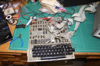
As received, the Superboard II produced garbage on the video output. I decided to take it back to factory configuration, since I had no documentation for the user modifications, and they were in poor shape. All of the extra wiring came off, and the board was set up per the manual. Still nothing useful on video! This is one of those systems where I find it pays to pull out the logic analyzer early, so one of our HP 1650A analyzers was set up from the start. Here it is, cabled to the Superboard II:
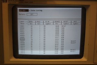
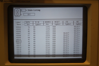
Quite the pile of wires! Most of them run to an A&P/3M 40 pin DIP clip, which grabs the 6502 processor. There are a few flying leads with grabbers that pick up other signals from the board, such as the boot ROM chip select. I copied one of my saved 6502 machine definitions and created an OSI 600 specific one. Here’s a look at the state listing just after a reset, while still in non-working condition:
We can see that the 6502 is attempting to fetch data from the boot ROM, and that the ROM is selecting and providing a reset vector. The 6502 then vectors to that address. This shows our first problem: the reset vector in the standard Superboard II boot ROM is supposed to be 0xFF00, but we’re seeing the 6502 pulling 0xDF00. Hmmm, time to burn a test ROM…
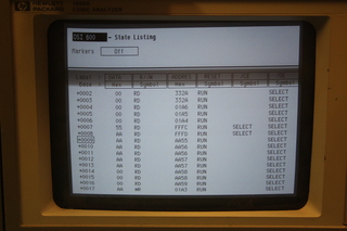
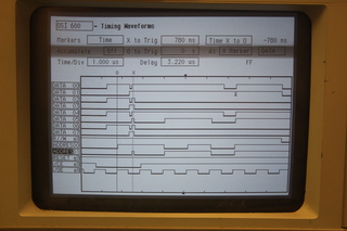
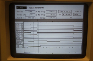
The test ROM contains a repeating pattern of 0xAA 0x55 – there’s no point in putting real 6502 code in at this point, since something is fundamentally broken. We can see the 6502 pulling 0xAA55 as the reset vector, and then jumping to it, but since it runs off into non-existent memory, we’re seeing the address mirrored onto the data bus. Let’s look at a timing capture for this access:
Ah, that’s not right! There’s a bunch of noise on the data lines, and it’s coincident with a problem on address bit 1. The 6502 was changed with a known-good CPU before the logic analyzer was even connected, so we know it’s not the 6502 itself having issues. With basically all devices that use the address and data bus removed except the test ROM and associated decode logic, the problem persisted. That pretty well means it must be a board issue, and given the quality of the modifications the Superboard II had when it arrived, that wouldn’t be surprising.
Sure enough, several top-side solder bridges were found at or near memory sockets. It looks like someone probably tried to tack onto traces on the top side of the board to expand system memory, which was a pretty common modification for the Superboard II. The sockets were removed and the shorts cleared. Now the timing capture looks like this:
That looks much more promising! Let’s put the OSI boot ROM back in and see what the state listing looks like:
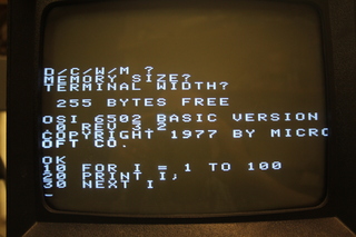
We can now see that the 6502 pulls 0xFF00 for the reset vector, and that 0xFF00 contains real data. 1K of system RAM in two 2114-type devices was installed, as well as the BASIC ROMs. Now on reset, we get this:
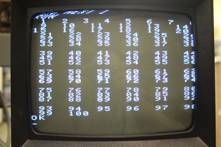
Success! Not much available RAM of course, but enough to print some numbers to the screen:
The little Ikegami test monitor is mis-adjusted for the Superboard II, but the system is now functional. This Superboard II is going to get a copy of CEGMON in a 2716 EPROM, the onboard memory maximized, and a few other modifications. For now, it runs well with the stock OSI boot ROM and ROM BASIC.
solder bridges cleared
