Topic: IMSAI SIO2 Modifications for MITS Disk System Compatibility
Date: 2022 JUN 25
A customer recently ordered a completely refurbished IMSAI system and wanted the system customized to run common IMSAI software, using the IMSAI SIO2 serial interface:
The customer also wanted customization to include a disk controller; specifically, DeRamp’s FDC+, an excellent replacement for MITS’ two-board disk controller. Unfortunately, the IMSAI SIO2 and MITS Disk Controller (and therefore, FDC+) have an I/O address conflict when set for standard/default addressing. The customer really wanted both at their defaults though, to preserve software compatibility with IMSAI programs and with utilities written for the MITS Disk Controller.
After reviewing the IMSAI SIO2 schematics, it was determined that the only I/O addressing overlap between the two is due to the SIO2’s control register. The control register is used to configure interrupts and carrier detect functionality. Very little software makes use of these features, and the customer decided to go for disabling the control register, if possible.

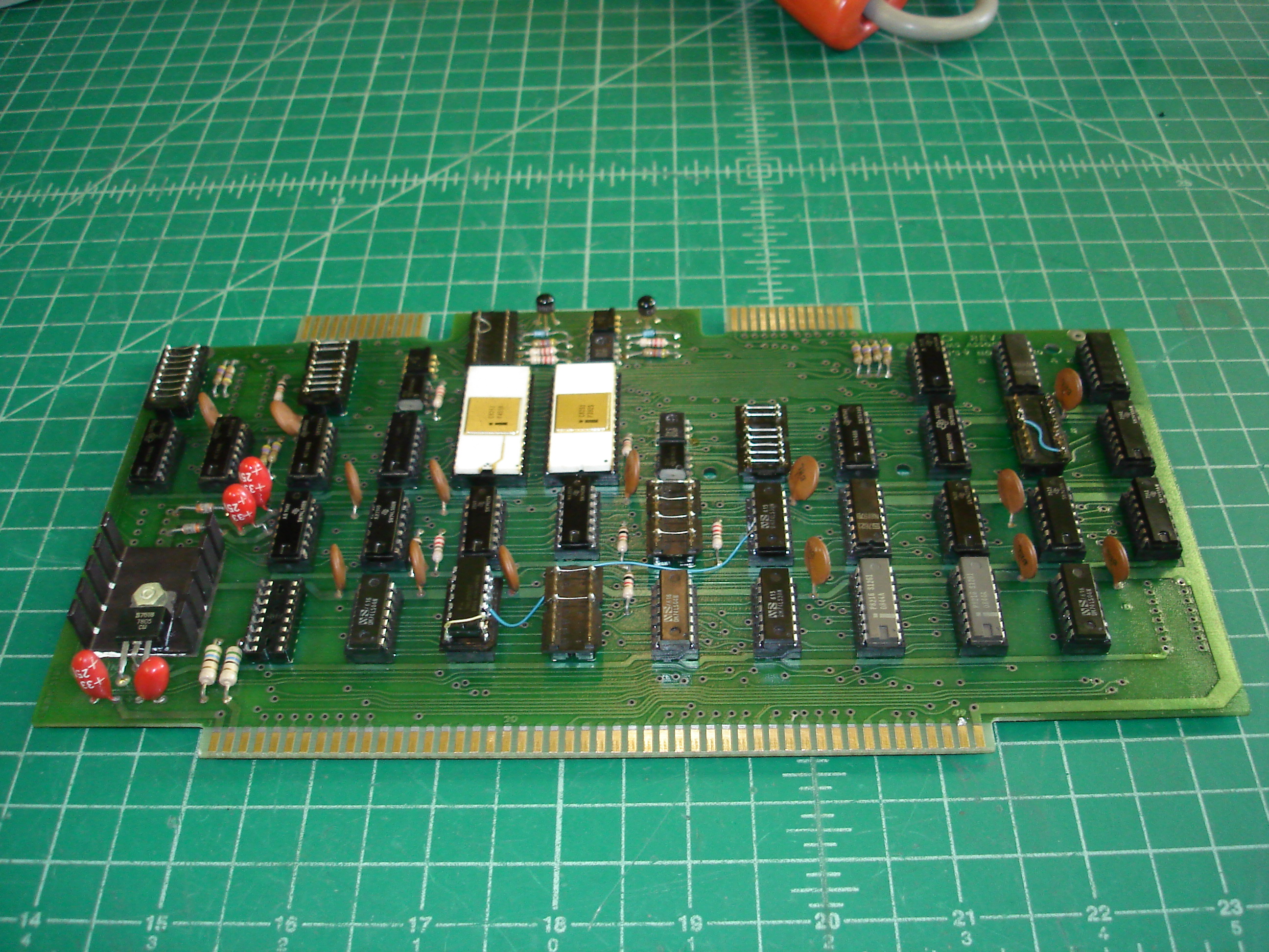
The modification turned out to be pretty simple: pull the active-low signal to enable the command register and buffer high, invert the A3 address line, and feed it into an unused input on a 74LS30 eight-input NAND gate. Further, it’s possible to achieve this without cutting any traces on the SIO2! Using a 14-pin DIP header, mount a 74LS00 “in the air,” with pins two and three cut off:


Pin 2 of the 74LS00 IC should be jumped to 5V, conveniently located on pin 14. Pin 3 on the DIP header must also be pulled to 5V, this was accomplished with a jumper underneath the 74LS00, installed before the 74LS00 was mounted on the DIP header. The inverted A3 signal is taken from pin 3 of the 74LS00, and run to pin 12 of the 74LS30. Pin 12 of the 74LS30 should be bent out so that it does not enter the socket:

This completes the modification. The socketed chips can be removed and replaced with non-modified chips at any time to restore original functionality. With the modification in place, serial channel A will appear at 0x02 and 0x03, and channel B will appear at 0x04 and 0x05, the same as an unmodified SIO2. The control register will not be accessible at any address, and will not conflict with the MITS disk controller or FDC+.
serial boards modified