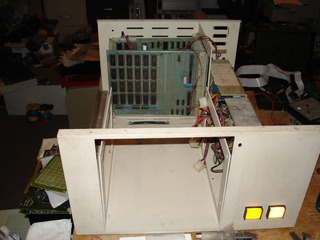
Topic: Getting the Challenger III online
Date: 2016 APR 20
About six years ago I found an Ohio Scientific Challenger III in the warehouse of a previous employer, dragged it into the shop, and started working on it. The boss had a kit-built Challenger III as their first business computer, and this one was a leftover from a previous business partner. Fortunately, he still had most of the manuals and software kicking around. Between the two systems, I was able to cobble together a single working Challenger III with 510 triple CPU board, 48K of RAM, a 470 floppy interface, and 8” disk drives.
The Challenger III got a bit of hobby use over the years, eventually getting upgraded to a single 48K 524 board, which uses much more reliable (and available) 2K x 8 6116 static RAMs. One of the 16K 520 boards was restrapped for 8K at 0xD000 - 0xE000 for CP/M, and I was finally able to (sort of) boot the CP/M 1.4 disks that came with the system. The Challenger III was set aside for other projects since it occupied so much space.
I decided to dig it out and get it going earlier this week, in order to work on a few OSI projects I’d shelved over the years. Apparently it was one of the systems in the front room when our contractor removed an old, unused chimney from the house – without covering any of the old fireplaces! There was a thick coating of soot and lime mortar dust all over the inside. Powering it up without cleaning wasn’t an option at all, so I stripped it completely down for a cleaning.
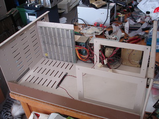
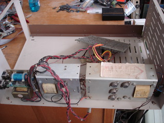
I didn’t think to take pictures of the original mess, but it went outside for an immediate vacuuming and blow-out with compressed air. All boards were removed, vacuumed, cleaned with a brush, then blown out. I removed the backplane, power supplies, and removable metal brackets from the case. The metal bits were all washed with soap and water. I finally thought to take pictures when the power supplies were back in:
Notice that the chassis rail is removed from the closest side – it’s much easier to work around the power supplies with it removed. It’s responsible for a fair bit of stiffening on the chassis though, so make sure it’s well supported. Apparently Ohio Scientific applied a dab of some sort of rubber adhesive when they assembled the chassis, so not only was it difficult to remove fasteners, but they then had to be cleaned before reuse.
While I had the chassis rail off, I increased the clearance between the power switch and the rearmost power supply. There was insufficient clearance to uninsulated 120 VAC for my liking. This is after the increase in clearance:
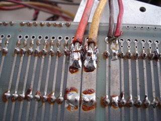
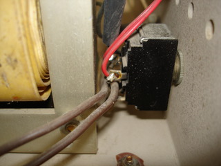
While I was in there, I went ahead and fixed the +5 and GND lines going to the backplane. The solder was sort of globbed on, typically a sign that the assembler was using a too-small iron. Interesting, as this was a factory assembled unit!
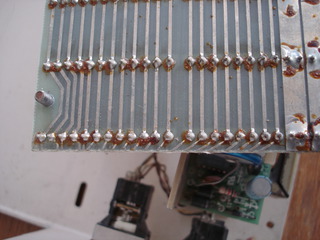
It seems that the 8-slot backplane was made by cutting down a larger backplane:
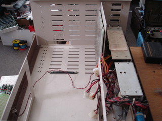
Finally reassembled! Here’s a few pictures before card installation:
This system had been working before storage and our move from New York. The power supplies checked out and were within spec on DC voltage and AC ripple. After cleaning and reassembly, with just the 510 CPU and 524 48K RAM boards installed, the system booted to the H/D/M? prompt! I went ahead and replaced the two burned out lamps in the front panel switches – I’d ordered a box of ten 330 type miniature lamps a few years ago but never got around to installing them. Here’s a picture of the system up and running:
I sorted through the 510 CPU board schematics in an effort to try and determine which pins on the AX connector were for reset, RS-232, and current loop. I went ahead and made a little ASCII art explanation of their location and function:
  Top left edge of 510 board, mounted, as seen from front

       ____   ____________
   ___|    |_|            |____________________________
  |    1  1   1 AX CONN  1                           B |
  |    3  6              2                           U |
  |                                                  S |

  The reset/console connector is designated "AX" in the OSI 510 schematics.

  Connector pinout:

  1     NC
  2     Reset Switch GND
  3     Reset Switch
  4     NC
  5     NC
  6     RS-232 GND
  7     RS-232 TX
  8     RS-232 RX
  9     20 mA TX+ (+5V loop supply)
  10    20 mA RX+
  11    20 mA TX-
  12    20 mA RX- (-9V loop supply)

  The little 4-pin connector is also counted as part of the AX connector. Its
  function relates to triple-processor selection. From the 510 schematics, it
  looks like it can be used for either an external switch (pull lines to ground)
  or to drive (buffered) indicators to show the active CPU under software
  control:

  13    GND
  14    /PSa (6502)
  15    /PSb (6800)
  16    /PSc (Z-80)
I’m using RS-232 on my setup, so no rejumpering of the 510 board was required. With the system up and running, I wanted to dump the ROMs installed on the board. Being a serial system, this OSI uses the 65A monitor, which is very different from the 65V monitor used on video-based OSI computers. The instruction manual for both monitors has been uploaded here. Additionally, my 510 board has the 68A2 monitor ROM installed, which is the same as the 400 board’s 68A monitor except generated for 0xFF00 - 0xFFFF. That manual is available here. Both sets of scans are from the original documentation that came with the boss’s machine.
In trying to dump the ROM monitors with the built-in 65A monitor, I got confused as to which ROM was where, as I had blank memory at 0xFD00 - 0xFDFF. I made another little ASCII art to help with this:
  6502 ROMs:

    __  __  __  __  __  __  __  __
   |  \/  ||  \/  ||  \/  ||  \/  |
   | FD00 || FE00 || FF00 ||      |
   |      ||      ||      ||      |
   | HD   || 65A  || BOOT || 6502 |
   |      ||      ||      ||      |
   |______||______||______||      |
                           |      |
                           |      |
                           |      |
                           |______|

  The 6800 ROM is the first 24-pin socket to the left of the Motorola 6800.
  It's at 0xFF00 when the 6800 is switched in.
I dumped the ROMs and converted them to binary files, they’re available here in binary form. I dropped the 6502 ROMs into mass:werk’s JavaScript 6502 disassembler and had a look at what was going on.
It appears that the boot ROM in my 510 board, located in the socket closest to the 6502 (addresses 0xFF00 - 0xFFFF) is responsible for initializing the system and signing on with the H/D/M? prompt. Apparently it checks the byte at 0xFE01 and assumes a serial system if it is 0x00. The boot prompt works as follows:
- Jump to
0xFD00if you select ‘H’ (hard disk boot) - Jump to
0xFF00if you select ‘D’ (floppy boot) - Jump indirect to the address at
0xFEFCfor any other input
0xFEFC is the “reset vector” (if the ROM were located at 0xFF00) in the 65A ROM monitor. Jumping to the address stored at 0xFEFC starts the monitor. In my 65A ROM, this location points to 0xFE35, which agrees with the manual as the 65A reset address. Presumably one could place anything else at 0xFD00 and jump to it with the ‘H’ command, as the ROM isn’t required to be present in OSI systems that don’t have a hard drive (there’s no ROM installed at this location in my Challenger III).
![["Cold solder joints", "Repaired solder joints"]](/~glitch/images/osi/challenger_3_cleanup/scaled/power_cold_solder.jpg)
